ZHCSOO1D December   2000  – August 2021 DCR021205 , DCR022405

PRODUCTION DATA  

  1. 特性
  2. 应用
  3. 说明
  4. Revision History
  5. Pin Configuration and Functions
  6. Specifications
    1. 6.1 Absolute Maximum Ratings
    2. 6.2 ESD Ratings
    3. 6.3 Recommended Operating Conditions
    4. 6.4 Thermal Information
    5. 6.5 Electrical Characteristics
    6. 6.6 Typical Characteristics
  7. Detailed Description
    1. 7.1 Overview
    2. 7.2 Functional Block Diagram
    3. 7.3 Feature Description
      1. 7.3.1 Isolation
        1. 7.3.1.1 Operation or Functional Isolation
        2. 7.3.1.2 Basic or Enhanced Isolation
        3. 7.3.1.3 Working Voltage
        4. 7.3.1.4 Isolation Voltage Rating
        5. 7.3.1.5 Repeated High-Voltage Isolation Testing
      2. 7.3.2 Power Stage
      3. 7.3.3 Oscillator and Watchdog
      4. 7.3.4 ERROR Flag
      5. 7.3.5 Synchronization
      6. 7.3.6 Construction
      7. 7.3.7 Decoupling – Ripple Reduction
    4. 7.4 Device Functional Modes
      1. 7.4.1 Device Disable and Enable
      2. 7.4.2 Regulated Output Disable and Enable
  8. Application and Implementation
    1. 8.1 Application Information
      1. 8.1.1 DCR02 Single Voltage Output
      2. 8.1.2 Generating Two Positive Output Voltages
      3. 8.1.3 Generation of Dual Polarity Voltages from Two Self-Synchronized DCR02s
    2. 8.2 Typical Application
      1. 8.2.1 Design Requirements
      2. 8.2.2 Detailed Design Procedure
        1. 8.2.2.1 Input Capacitor
        2. 8.2.2.2 Output Capacitor
        3. 8.2.2.3 Filter Capacitor
        4. 8.2.2.4 ERROR Flag
      3. 8.2.3 Application Curves
  9. Power Supply Recommendations
  10. 10Layout
    1. 10.1 Layout Guidelines
    2. 10.2 Layout Examples
    3. 10.3 Thermal Consideration
  11. 11Device and Documentation Support
    1. 11.1 Documentation Support
      1. 11.1.1 Related Documentation
    2. 11.2 接收文档更新通知
    3. 11.3 支持资源
    4. 11.4 Trademarks
    5. 11.5 Electrostatic Discharge Caution
    6. 11.6 术语表
  12. 12Mechanical, Packaging, and Orderable Information

封装选项

机械数据 (封装 | 引脚)
散热焊盘机械数据 (封装 | 引脚)
订购信息

Pin Configuration and Functions

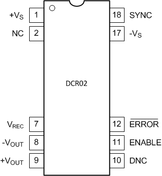
GUID-4B9031F9-7B9F-4569-924E-21A78C9FF3B0-low.gifFigure 5-1 NVE or DVS Package10-Pin PDIP or SOPTop View
Table 5-1 Pin Functions
PIN I/O(1) DESCRIPTION
NO. NAME
1 +VS I Voltage input
2 NC No connection
7 VREC O Rectified output
8 –VOUT O Output ground
9 +VOUT O Voltage output
10 DNC Do not connect
11 ENABLE I Output voltage enable
12 ERROR O Error flag active low
17 –VS I Input ground
18 SYNC I Synchronization input
I = input and O = output