SCAS871H February 2009 – January 2016 CDCM61004
PRODUCTION DATA.
- 1 Features
- 2 Applications
- 3 Description
- 4 Revision History
- 5 Description (Continued)
- 6 Pin Configuration and Functions
-
7 Specifications
- 7.1 Absolute Maximum Ratings
- 7.2 ESD Ratings
- 7.3 Recommended Operating Conditions
- 7.4 Thermal Information
- 7.5 Electrical Characteristics
- 7.6 Typical Output Phase Noise CharacteristicsCorrected units for tRJIT (RMS phase jitter); changed to fs, RMS from ps, RMS
- 7.7 Typical Output Jitter Characteristics
- 7.8 Crystal Characteristics
- 7.9 Dissipation Ratings
- 7.10 Typical Characteristics
- 8 Parameter Measurement Information
-
9 Detailed Description
- 9.1 Overview
- 9.2 Functional Block Diagram
- 9.3
Feature Description
- 9.3.1 Phase-Locked Loop (PLL)
- 9.3.2 Configuring the PLL
- 9.3.3 Crystal Input Interface
- 9.3.4 Phase Frequency Detector (PFD)
- 9.3.5 Charge Pump (CP)
- 9.3.6 On-Chip PLL Loop Filter
- 9.3.7 Prescaler Divider and Feedback Divider
- 9.3.8 On-Chip VCO
- 9.3.9 LVCMOS Input Interface
- 9.3.10 Output Divider
- 9.3.11 Output Buffer
- 9.4 Device Functional Modes
- 10Application and Implementation
- 11Power Supply Recommendations
- 12Layout
- 13Device and Documentation Support
- 14Mechanical, Packaging, and Orderable Information
7 Specifications
7.1 Absolute Maximum Ratings
Over operating free-air temperature range (unless otherwise noted).(1)| PARAMETER | MIN | MAX | UNIT | ||
|---|---|---|---|---|---|
| VCC | Supply voltage(2) | VCC_OUT, | –0.5 | 4.6 | V |
| VCC_PLL1 | |||||
| VCC_PLL2 | |||||
| VCC_VCO | |||||
| VCC_IN | |||||
| VIN | Input voltage(3) | –0.5 | VCC_IN + 0.5 | V | |
| VOUT | Output voltage range(3) | –0.5 | VCC_OUT + 0.5 | V | |
| IN | Input current | –20 | 20 | mA | |
| IOUT | Output current | –50 | 50 | mA | |
| Tstg | Storage temperature | –65 | 150 | °C | |
(1) Stresses beyond those listed under Absolute Maximum Ratings may cause permanent damage to the device. These are stress ratings only, and functional operation of the device at these or any other conditions beyond those indicated under Recommended Operating Conditions is not implied. Exposure to absolute-maximum-rated conditions for extended periods may affect device reliability.
(2) All supply voltages must be supplied simultaneously.
(3) Input and output negative voltage ratings may be exceeded if the input and output clamp-current ratings are observed.
7.2 ESD Ratings
| VALUE | UNIT | |||
|---|---|---|---|---|
| V(ESD) | Electrostatic discharge | Human-body model (HBM), per ANSI/ESDA/JEDEC JS-001(1) | ±3000 | V |
| Charged-device model (CDM), per JEDEC specification JESD22-C101(2) | ±1000 | |||
(1) JEDEC document JEP155 states that 500-V HBM allows safe manufacturing with a standard ESD control process. Manufacturing with less than 500-V HBM is possible with the necessary precautions.
(2) JEDEC document JEP157 states that 250-V CDM allows safe manufacturing with a standard ESD control process. Manufacturing with less than 250-V CDM is possible with the necessary precautions.
7.3 Recommended Operating Conditions
Over operating free-air temperature range (unless otherwise noted).| MIN | NOM | MAX | UNIT | |||
|---|---|---|---|---|---|---|
| VCC_OUT | Output supply voltage | 3 | 3.3 | 3.6 | V | |
| VCC_PLL1 | PLL supply voltage | 3 | 3.3 | 3.6 | V | |
| VCC_PLL2 | PLL supply voltage | 3 | 3.3 | 3.6 | V | |
| VCC_VCO | On-chip VCO supply voltage | 3 | 3.3 | 3.6 | V | |
| VCC_IN | Input supply voltage | 3 | 3.3 | 3.6 | V | |
| TA | Ambient temperature | –40 | 85 | °C | ||
| |TCL| | Allowable temperature drift for continuous PLL lock(1) | 100 | °C | |||
(1) The maximum allowable temperature drift for continuous lock is how far the temperature can drift in either direction from the value it was at the time when the On-Chip VCO was calibrated with the condition that the PLL stays in lock throughout the temperature drift. The internal VCO calibration takes place at device start-up and when the device is reset using the RSTN pin. A more detailed description can be found in On-Chip VCO and Start-Up Time Estimation.This implies the part will work over the entire frequency range, but if the temperature drifts more than the maximum allowable temperature drift for continuous lock, then it is necessary to re-calibrate the VCO to ensure the PLL stays in lock. Regardless of what temperature the part was initially calibrated at, the temperature can never drift outside the ambient temperature range of –40 °C to 85 °C.
7.4 Thermal Information
| THERMAL METRIC(1) | CDCM61004 | UNIT | |
|---|---|---|---|
| RHB (VQFN) | |||
| 32 PINS | |||
| RθJA | Junction-to-ambient thermal resistance | 33.1 | °C/W |
| RθJC(top) | Junction-to-case (top) thermal resistance | 25.7 | °C/W |
| RθJB | Junction-to-board thermal resistance | 0.3 | °C/W |
| ψJT | Junction-to-top characterization parameter | 7.1 | °C/W |
| ψJB | Junction-to-board characterization parameter | 2 | °C/W |
| RθJC(bot) | Junction-to-case (bottom) thermal resistance | 6.12 | °C/W |
(1) For more information about traditional and new thermal metrics, see the Semiconductor and IC Package Thermal Metrics application report, SPRA953.
7.5 Electrical Characteristics
At VCC = 3 V to 3.6 V and TA = –40°C to 85°C, unless otherwise noted.| PARAMETER | TEST CONDITIONS | MIN | TYP | MAX | UNIT | |
|---|---|---|---|---|---|---|
| CONTROL PIN LVCMOS INPUT CHARACTERISTICS | ||||||
| VIH | Input high voltage | 0.6 VCC | V | |||
| VIL | Input low voltage | 0.4 VCC | V | |||
| IIH | Input high current | VCC = 3.6 V, VIL = 0 V | 200 | μA | ||
| IIL | Input low current | VCC = 3 V, VIH = 3.6 V | –200 | μA | ||
| LVCMOS OUTPUT CHARACTERISTICS(1) (See Figure 7 and Figure 8) | ||||||
| fOSC_OUT | Bypass output frequency | 21.875 | 28.47 | MHz | ||
| fOUT | Output frequency | 43.75 | 250 | MHz | ||
| VOH | Output high voltage | VCC = min to max, IOH = –100 μA | VCC –0.5 | V | ||
| VOL | Output low voltage | VCC = min to max, IOL = 100 μA | 0.3 | V | ||
| tRJIT | RMS phase jitter | 250 MHz (10 kHz to 20 MHz) | 0.85 | ps, RMS | ||
| tSLEW-RATE | Output rise/fall slew rate | 20% to 80% | 2.4 | V/ns | ||
| ODC | Output duty cycle | 45% | 55% | |||
| tSKEW | Skew between outputs | 60 | ps | |||
| ICC, LVCMOS | Device current, LVCMOS | fIN = 25 MHz, fOUT = 250 MHz, CL = 5 pF | 175 | 205 | mA | |
| LVPECL OUTPUT CHARACTERISTICS(2) (See Figure 9 and Figure 10) | ||||||
| fOUT | Output frequency | 43.75 | 683.264 | MHz | ||
| VOH | Output high voltage | VCC –1.18 | VCC –0.73 | V | ||
| VOL | Output low voltage | VCC –2 | VCC –1.55 | V | ||
| |VOD| | Differential output voltage | 0.6 | 1.23 | V | ||
| tRJIT | RMS phase jitter | 625 MHz (10 kHz to 20 MHz) | 0.77 | ps, RMS | ||
| tR/tF | Output rise/fall time | 20% to 80% | 175 | ps | ||
| ODC | Output duty cycle | 45% | 55% | |||
| tSKEW | Skew between outputs | 30 | ps | |||
| ICC, LVPECL | Device current, LVPECL | fIN = 25 MHz, fOUT = 625 MHz | 180 | 215 | mA | |
| LVDS OUTPUT CHARACTERISTICS(3) (See Figure 11 and Figure 12) | ||||||
| fOUT | Output frequency | 43.75 | 683.264 | MHz | ||
| |VOD| | Differential output voltage | 0.247 | 0.454 | V | ||
| ΔVOD | VDD magnitude change | 50 | mV | |||
| VOS | Common-mode voltage | 1.125 | 1.375 | V | ||
| ΔVOS | VOS magnitude change | 50 | mV | |||
| tRJIT | RMS phase jitter | 625 MHz (10 kHz to 20 MHz) | 0.73 | ps, RMS | ||
| tR/tF | Output rise/fall time | 20% to 80% | 255 | ps | ||
| ODC | Output duty cycle | 45% | 55% | |||
| tSKEW | Skew between outputs | 40 | ps | |||
| ICC, LVDS | Device current, LVDS | fIN = 25 MHz, fOUT = 625 MHz | 150 | 195 | mA | |
(1) Figure 7 and Figure 8 show DC and AC test setups, respectively. Jitter measurements made using 25-MHz quartz crystal inches.
7.6 Typical Output Phase Noise Characteristics
Over operating free-air temperature range (unless otherwise noted).| PARAMETER | TEST CONDITIONS | MIN | TYP | MAX | UNIT | |
|---|---|---|---|---|---|---|
| 250-MHz LVCMOS OUTPUT(1) (See Figure 8) | ||||||
| phn100 | Phase noise at 100-Hz offset | –95 | dBc/Hz | |||
| phn1k | Phase noise at 1-kHz offset | –110 | dBc/Hz | |||
| phn10k | Phase noise at 10-kHz offset | –117 | dBc/Hz | |||
| phn100k | Phase noise at 100-kHz offset | –120 | dBc/Hz | |||
| phn1M | Phase noise at 1-MHz offset | –135 | dBc/Hz | |||
| phn10M | Phase noise at 10-MHz offset | –148 | dBc/Hz | |||
| phn20M | Phase noise at 20-MHz offset | –148 | dBc/Hz | |||
| tRJIT | RMS phase jitter from 10 kHz to 20 MHz | 544 | fs, RMS | |||
| tPJIT | Total period jitter | 27.4 | ps, PP | |||
| tSTARTUP | Start-up time, power supply ramp time of 1 ms, final frequency accuracy of ±10 ppm |
2.25 | ms | |||
| 625-MHz LVPECL OUTPUT(2) (See Figure 10) | ||||||
| phn100 | Phase noise at 100-Hz offset | –81 | dBc/Hz | |||
| phn1k | Phase noise at 1-kHz offset | –101 | dBc/Hz | |||
| phn10k | Phase noise at 10-kHz offset | –109 | dBc/Hz | |||
| phn100k | Phase noise at 100-kHz offset | –112 | dBc/Hz | |||
| phn1M | Phase noise at 1-MHz offset | –129 | dBc/Hz | |||
| phn10M | Phase noise at 10-MHz offset | –146 | dBc/Hz | |||
| phn20M | Phase noise at 20-MHz offset | –146 | dBc/Hz | |||
| tRJIT | RMS phase jitter from 10 kHz to 20 MHz | 509 | fs, RMS | |||
| tPJIT | Total period jitter | 26.9 | ps, PP | |||
| tSTARTUP | Start-up time, power supply ramp time of 1 ms, final frequency accuracy of ±10 ppm |
2.25 | ms | |||
| 625-MHz LVDS OUTPUT(3) (See Figure 12) | ||||||
| phn100 | Phase noise at 100-Hz offset | –88 | dBc/Hz | |||
| phn1k | Phase noise at 1-kHz offset | –102 | dBc/Hz | |||
| phn10k | Phase noise at 10-kHz offset | –109 | dBc/Hz | |||
| phn100k | Phase noise at 100-kHz offset | –112 | dBc/Hz | |||
| phn1M | Phase noise at 1-MHz offset | –129 | dBc/Hz | |||
| phn10M | Phase noise at 10-MHz offset | –146 | dBc/Hz | |||
| phn20M | Phase noise at 20-MHz offset | –146 | dBc/Hz | |||
| tRJIT | RMS phase jitter from 10 kHz to 20 MHz | 510 | fs, RMS | |||
| tPJIT | Total period jitter | 27 | ps, PP | |||
| tSTARTUP | Start-up time, power supply ramp time of 1 ms, final frequency accuracy of ±10 ppm |
2.25 | ms | |||
(1) Figure 8 shows test setup and uses 25-MHz quartz crystal in, VCC = 3.3 V, and TA = 25°C.
(2) Figure 10 shows test setup and uses 25-MHz quartz crystal in, VCC = 3.3 V, and TA = 25°C.
(3) Figure 12 shows test setup and uses 25-MHz quartz crystal in, VCC = 3.3 V, and TA = 25°C.
7.7 Typical Output Jitter Characteristics(1)
| OUTPUT FREQUENCY (MHz) |
INPUT (MHz) | LVCMOS OUTPUT | LVPECL OUTPUT | LVDS OUTPUT | |||
|---|---|---|---|---|---|---|---|
| tRJIT (fs, RMS) | tPJIT (psPP) | tRJIT (fs, RMS) | tPJIT (psPP) | tRJIT (fs, RMS) | tPJIT (psPP) | ||
| 62.5 | 25 | 592 | 32.9 | 611 | 20.7 | 667 | 28.4 |
| 75 | 25 | 518 | 27.5 | 533 | 19.4 | 572 | 25.7 |
| 77.76 | 24.8832 | 506 | 29.2 | 526 | 20.9 | 567 | 26.9 |
| 100 | 25 | 507 | 24.5 | 510 | 20.7 | 533 | 26.5 |
| 106.25 | 26.5625 | 535 | 23.5 | 524 | 20.2 | 553 | 26.5 |
| 125 | 25 | 557 | 39.6 | 556 | 21.4 | 570 | 27.1 |
| 150 | 25 | 518 | 38.4 | 493 | 18.9 | 515 | 26.2 |
| 155.52 | 24.8832 | 498 | 36.9 | 486 | 19.8 | 502 | 26.7 |
| 156.25 | 25 | 510 | 37.7 | 503 | 20.7 | 518 | 26.5 |
| 159.375 | 26.5625 | 535 | 37.4 | 510 | 19.9 | 534 | 26.3 |
| 187.5 | 25 | 506 | 32.8 | 506 | 20.3 | 509 | 25.5 |
| 200 | 25 | 491 | 23.3 | 492 | 30 | 499 | 34.9 |
| 212.5 | 26.5625 | 520 | 47.8 | 509 | 30.8 | 530 | 37.3 |
| 250 | 25 | 544 | 27.4 | 541 | 21.4 | 550 | 27.5 |
| 311.04 | 24.8832 | 481 | 20.5 | 496 | 24.7 | ||
| 312.5 | 25 | 501 | 20.8 | 508 | 25.8 | ||
| 622.08 | 24.8832 | 492 | 27.2 | 500 | 27.2 | ||
| 625 | 25 | 515 | 26.9 | 509 | 27 | ||
7.8 Crystal Characteristics
7.9 Dissipation Ratings(1)(2)
| PARAMETER | TEST CONDITIONS |
VALUE | UNIT | |
|---|---|---|---|---|
| 4 × 4 VIAS ON PAD |
||||
| θJA | Thermal resistance, junction-to-ambient | 0 LFM | 35 | °C/W |
| θJP(3) | Thermal resistance, junction-to-pad | 4 | °C/W | |
(1) The package thermal resistance is calculated in accordance with JESD 51 and JEDEC 2S2P (high-K board).
(2) Connected to GND with nine thermal vias (0.3-mm diameter).
(3) θJP (junction-to-pad) is used for the VQFN package, because the primary heat flow is from the junction to the GND pad of the VQFN package.
7.10 Typical Characteristics
Over operating free-air temperature range (unless otherwise noted).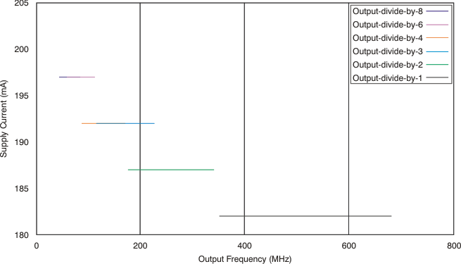 Figure 1. Typical Current Consumption for LVPECL Output vs Output Frequency
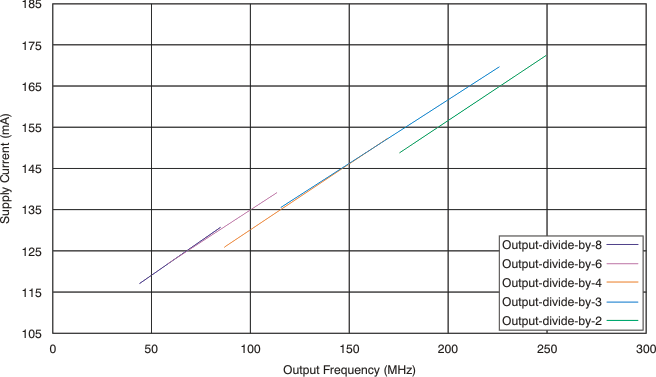 Figure 3. Typical Current Consumption for LVCMOS Output With 5-pF Load vs Output Frequency
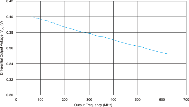 Figure 5. Typical LVDS Differential Output Voltage vs Output Frequency
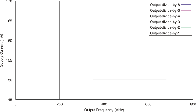 Figure 2. Typical Current Consumption for LVDS Output vs Output Frequency
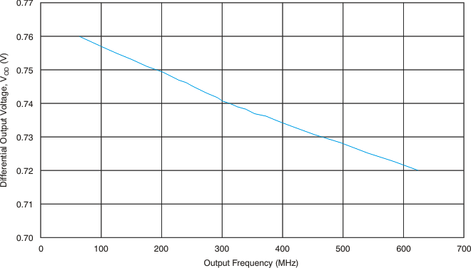 Figure 4. Typical LVPECL Differential Output Voltage vs Output Frequency
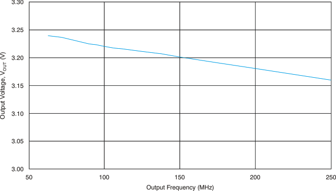 Figure 6. Typical LVCMOS Output Voltage With 5-pF Load vs Output Frequency