SCAS871H February 2009 – January 2016 CDCM61004
PRODUCTION DATA.
- 1 Features
- 2 Applications
- 3 Description
- 4 Revision History
- 5 Description (Continued)
- 6 Pin Configuration and Functions
-
7 Specifications
- 7.1 Absolute Maximum Ratings
- 7.2 ESD Ratings
- 7.3 Recommended Operating Conditions
- 7.4 Thermal Information
- 7.5 Electrical Characteristics
- 7.6 Typical Output Phase Noise CharacteristicsCorrected units for tRJIT (RMS phase jitter); changed to fs, RMS from ps, RMS
- 7.7 Typical Output Jitter Characteristics
- 7.8 Crystal Characteristics
- 7.9 Dissipation Ratings
- 7.10 Typical Characteristics
- 8 Parameter Measurement Information
-
9 Detailed Description
- 9.1 Overview
- 9.2 Functional Block Diagram
- 9.3
Feature Description
- 9.3.1 Phase-Locked Loop (PLL)
- 9.3.2 Configuring the PLL
- 9.3.3 Crystal Input Interface
- 9.3.4 Phase Frequency Detector (PFD)
- 9.3.5 Charge Pump (CP)
- 9.3.6 On-Chip PLL Loop Filter
- 9.3.7 Prescaler Divider and Feedback Divider
- 9.3.8 On-Chip VCO
- 9.3.9 LVCMOS Input Interface
- 9.3.10 Output Divider
- 9.3.11 Output Buffer
- 9.4 Device Functional Modes
- 10Application and Implementation
- 11Power Supply Recommendations
- 12Layout
- 13Device and Documentation Support
- 14Mechanical, Packaging, and Orderable Information
9 Detailed Description
9.1 Overview
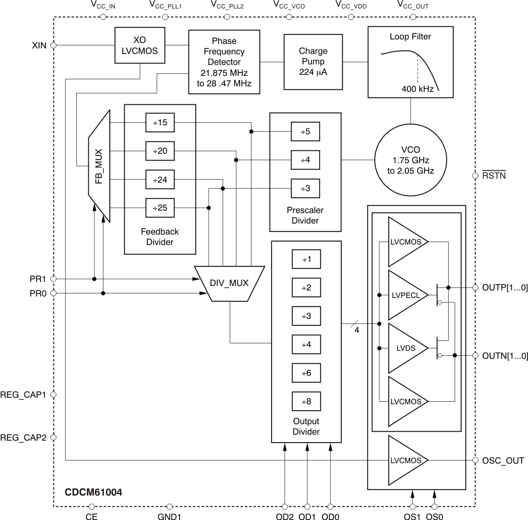
The CDCM61004 is a high-performance PLL that generates 4 copies of commonly used reference clocks with less than 1 ps, RMS jitter from a low-cost crystal.
9.2 Functional Block Diagram

9.3 Feature Description
9.3.1 Phase-Locked Loop (PLL)
The CDCM61004 includes an on-chip PLL with an on-chip VCO. The PLL blocks consist of a crystal input interface, which can also accept an LVCMOS signal, a phase frequency detector (PFD), a charge pump, an on-chip loop filter, and prescaler and feedback dividers. Completing the CDCM61004 device are the output divider and universal output buffer.
The PLL is powered by on-chip, low-dropout (LDO) linear voltage regulators. The regulated supply network is partitioned such that the sensitive analog supplies are powered from separate LDOs rather than the digital supplies which use a separate LDO regulator. These LDOs provide isolation for the PLL from any noise in the external power-supply rail. The REG_CAP1 and REG_CAP2 pins should each be connected to ground by 10-μF capacitors to ensure stability.
9.3.2 Configuring the PLL
The CDCM61004 permits PLL configurations to accommodate the various input and output frequencies listed in Table 2 and Table 3. These configurations are accomplished by setting the prescaler divider, feedback divider and output divider. The various dividers are managed by setting the device control pins as shown in Table 4 and Table 5.
9.3.3 Crystal Input Interface
Fundamental mode is the recommended oscillation mode of operation for the input crystal and parallel resonance is the recommended type of circuit for the crystal.
A crystal load capacitance refers to all capacitances in the oscillator feedback loop. It is equal to the amount of capacitance seen between the terminals of the crystal in the circuit. For parallel resonant mode circuits, the correct load capacitance is necessary to ensure the oscillation of the crystal within the expected parameters.
The CDCM61004 implements an input crystal oscillator circuitry, known as the Colpitts oscillator, and requires one pad of the crystal to interface with the XIN pin; the other pad of the crystal is tied to ground. In this crystal interface, it is important to account for all sources of capacitance when calculating the correct value for the discrete capacitor component, CL, for a design.
The CDCM61004 has been characterized with 10-pF parallel resonant crystals. The input crystal oscillator stage in the CDCM61004 is designed to oscillate at the correct frequency for all parallel resonant crystals with low-pull capability and rated with a load capacitance that is equal to the sum of the onchip load capacitance at the XIN pin (10-pF), crystal stray capacitance, and board parasitic capacitance between the crystal and XIN pin.
The normalized frequency error of the crystal, as a result of load capacitance mismatch, can be calculated as Equation 2:

where
- CS is the motional capacitance of the crystal,
- C0 is the shunt capacitance of the crystal,
- CL,R is the rated load capacitance for the crystal,
- CL,A is the actual load capacitance in the implemented PCB for the crystal,
- Δf is the frequency error of the crystal,
- and f is the rated frequency of the crystal.
- The first three parameters can be obtained from the crystal vendor.
To minimize the frequency error of the crystal to meet application requirements, the difference between the rated load capacitance and the actual load capacitance should be minimized and a crystal with low-pull capability (low CS) should be used.
For example, if an application requires less than ±50-ppm frequency error and a crystal with less than ±50-ppm frequency tolerance is picked, the characteristics are as follows: C0 = 7 pF, CS = 10 fF, and CL,R = 12 pF. In order to meet the required frequency error, calculate CL,A using Equation 2 to be 17 pF. Subtracting CL,R from CL,A, results in 5 pF; take care during printed-circuit-board (PCB) layout with the crystal and the CDCM61004 to ensure that the sum of the crystal stray capacitance and board parasitic capacitance is less than the calculated 5 pF.
Good layout practices are fundamental to the correct operation and reliability of the oscillator. It is critical to locate the crystal components very close to the XIN pin to minimize routing distances. Long traces in the oscillator circuit are a very common source of problems. Do not route other signals across the oscillator circuit. Also, make sure power and high-frequency traces are routed as far away as possible to avoid crosstalk and noise coupling. Avoid the use of vias; if the routing becomes very complex, it is much better to use 0-Ω resistors as bridges to go over other signals. Vias in the oscillator circuit should only be used for connections to the ground plane. Do not share ground connections; instead, make a separate connection to ground for each component that requires grounding. If possible, place multiple vias in parallel for each connection to the ground plane. Especially in the Colpitts oscillator configuration, the oscillator is very sensitive to capacitance in parallel with the crystal. Therefore, the layout must be designed to minimize stray capacitance across the crystal to less than 5 pF total under all circumstances to ensure proper crystal oscillation. Be sure to consider both PCB and crystal stray capacitance.
Table 1 lists several recommended crystals and the respective manufacturer of each.
Table 1. Recommended Crystal Manufacturers
| MANUFACTURER | PART NUMBER |
|---|---|
| Vectron | VXC1-1133 |
| Fox | 218-3 |
| Saronix | FP2650002 |
9.3.4 Phase Frequency Detector (PFD)
The PFD takes inputs from the input interface and the feedback divider and produces an output that depends on the phase and frequency differences between the two inputs. The allowable range of frequencies at the PFD inputs is 21.875 MHz to 28.47 MHz.
9.3.5 Charge Pump (CP)
The charge pump is controlled by the PFD, which dictates either to pump up or down to charge or discharge the integrating section of the on-chip loop filter. The integrated and filtered charge pump current is then converted to a voltage that drives the control voltage node of the internal VCO through the on-chip loop filter. The charge pump current is preset to 224 μA and cannot be changed.
9.3.6 On-Chip PLL Loop Filter
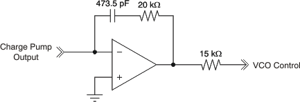
Figure 14 shows the on-chip active loop filter topology implemented in the device. This design corresponds to a PLL bandwidth of 400 kHz for a PFD in the range of 21.875 MHz to 28.47 MHz, and a charge pump current of 224 μA.
 Figure 14. On-Chip PLL Loop Filter Topology
9.3.7 Prescaler Divider and Feedback Divider
The VCO output is routed to the prescaler divider and then to the feedback divider. The prescaler divider and feedback divider are set in tandem with each other, according to the control pin settings given in Table 4. The allowable combinations of the two dividers ensure that the VCO frequency and the PFD frequency are within the specified limits.
9.3.8 On-Chip VCO
The CDCM61004 includes an on-chip, LC oscillator-based VCO with low phase noise covering a frequency range of 1.75 GHz to 2.05 GHz. The VCO must be calibrated to ensure proper operation over the valid device operating conditions. This calibration requires that the PLL be set up properly to lock the PLL loop and that the reference clock input be present. During the first device initialization after power-up, which occurs after the Power-On-Reset is released (2.64 V or lower, over valid device operating conditions) or a device reset with the RSTN pin, a VCO calibration sequence is initiated after 16,384 × Reference Input Clock Cycles. The VCO calibration then takes about 20 µs over the allowable range of the reference clock input.
The VCO calibration can also be reinitiated with a pulse on the RSTN pin at any time after POR is released on power-up; the RSTN pulse must be at least 100 ns wide.
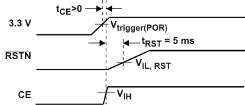
For proper device operation, the reference input must be stable at the start of VCO calibration. Since inputs from crystals or crystal oscillators can typically take up to 1-2ms to be stable, TI recommends to establish circuitry on the RSTN pin that ensures device initialization including VCO calibration after a delay of greater than 5 ms compared to the power-up ramp, as shown in Figure 15. A possible implementation of the delay circuitry on the RSTN pin would be a 47-nF capacitor to GND, and this in tandem with the 150-kΩ on-chip pullup resistor ensures the appropriate delay. The CE pin has an internal 150-kΩ pullup resistor and can be left unconnected or pulled to high for proper device operation.
The device can operate at temperatures within the ambient temperature range TA. Within the ambient temperature limits and after the point in time when the VCO calibrated, the absolute temperature drift must be smaller than the maximum allowable temperature drift for continuous lock |TCL| for the PLL to stay in lock to an appropriate input reference. When a larger absolute temperature drift has to be covered, the VCO needs to be re-calibrated as described above.
9.3.9 LVCMOS Input Interface
Alternately, the CDCM61004 can be operated with an external AC-coupled 2.5-V LVCMOS or DC-coupled 3.3-V LVCMOS reference input applied to the XIN pin. For proper operation, the LVCMOS reference should be available and fairly stable by the time the power supply voltages or the RSTN pin voltage on the CDCM61004 reaches 2.27 V. For more details about the LVCMOS input interface to the CDCM61004, see the application report, Using LVCMOS Input to the CDM6100x (SCAA111), available on ti.com.
9.3.10 Output Divider
The output from the prescaler divider is also routed to the output divider. The output divider can be set with control pins according to Table 5.
9.3.11 Output Buffer
Each output buffer can be set to LVPECL or LVDS or 2x LVCMOS, according to Table 6. OSC_OUT is an LVCMOS output that can be used to monitor proper loading of the input crystal to achieve the necessary crystal frequency with the least error. The OSC_OUT turns on as soon as power is available and remains on during deviec calibration. The output buffers are disabled during VCO calibration and are enabled only after calibration is complete.
The output buffers on the CDCM61004 can also be disabled, along with other sections of the device, using the CE pin according to Table 7.
9.4 Device Functional Modes
Table 2. Common Configuration
Table 3. Generic Configuration
| INPUT FREQUENCY RANGE (MHz) | PRESCALER DIVIDER | FEEDBACK DIVIDER | VCO FREQUENCY RANGE (MHz) | OUTPUT DIVIDER | OUTPUT FREQUENCY RANGE (MHz) |
|---|---|---|---|---|---|
| 21.875 to 25.62 | 4 | 20 | 1750 to 2050 | 8 | 54.6875 to 64.05 |
| 21.875 to 25.62 | 4 | 20 | 1750 to 2050 | 6 | 72.92 to 85.4 |
| 21.875 to 25.62 | 4 | 20 | 1750 to 2050 | 4 | 109.375 to 128.1 |
| 21.875 to 25.62 | 4 | 20 | 1750 to 2050 | 3 | 145.84 to 170.8 |
| 21.875 to 25.62 | 4 | 20 | 1750 to 2050 | 2 | 218.75 to 256.2 |
| 21.875 to 25.62 | 4 | 20 | 1750 to 2050 | 1 | 437.5 to 512.4 |
| 23.33 to 27.33 | 3 | 25 | 1750 to 2050 | 8 | 72.906 to 85.408 |
| 23.33 to 27.33 | 3 | 25 | 1750 to 2050 | 6 | 97.21 to 113.875 |
| 23.33 to 27.33 | 3 | 25 | 1750 to 2050 | 4 | 145.812 to 170.816 |
| 23.33 to 27.33 | 3 | 25 | 1750 to 2050 | 3 | 194.42 to 227.75 |
| 23.33 to 27.33 | 3 | 25 | 1750 to 2050 | 2 | 291.624 to 341.632 |
| 23.33 to 27.33 | 3 | 25 | 1750 to 2050 | 1 | 583.248 to 683.264 |
| 23.33 to 27.33 | 5 | 15 | 1750 to 2050 | 8 | 43.75 to 51.25 |
| 23.33 to 27.33 | 5 | 15 | 1750 to 2050 | 6 | 58.33 to 68.33 |
| 23.33 to 27.33 | 5 | 15 | 1750 to 2050 | 4 | 87.5 to 102.5 |
| 23.33 to 27.33 | 5 | 15 | 1750 to 2050 | 3 | 116.66 to 136.66 |
| 23.33 to 27.33 | 5 | 15 | 1750 to 2050 | 2 | 175 to 205 |
| 23.33 to 27.33 | 5 | 15 | 1750 to 2050 | 1 | 350 to 410 |
| 24.305 to 28.47 | 3 | 24 | 1750 to 2050 | 8 | 72.915 to 85.41 |
| 24.305 to 28.47 | 3 | 24 | 1750 to 2050 | 6 | 97.22 to 113.88 |
| 24.305 to 28.47 | 3 | 24 | 1750 to 2050 | 4 | 145.83 to 170.82 |
| 24.305 to 28.47 | 3 | 24 | 1750 to 2050 | 3 | 194.44 to 227.76 |
| 24.305 to 28.47 | 3 | 24 | 1750 to 2050 | 2 | 291.66 to 341.64 |
| 24.305 to 28.47 | 3 | 24 | 1750 to 2050 | 1 | 583.32 to 683.28 |
Table 4. Programmable Prescaler and Feedback Divider Settings
| CONTROL INPUTS | PRESCALER DIVIDER | FEEDBACK DIVIDER | PFD FREQUENCY | ||
|---|---|---|---|---|---|
| PR1 | PR0 | MIN | MAX | ||
| 0 | 0 | 3 | 24 | 24.305 | 28.47 |
| 0 | 1 | 5 | 15 | 23.33 | 27.33 |
| 1 | 0 | 3 | 25 | 23.33 | 27.33 |
| 1 | 1 | 4 | 20 | 21.875 | 25.62 |
Table 5. Programmable Output Divider
| CONTROL INPUTS | OUTPUT DIVIDER | ||
|---|---|---|---|
| OD2 | OD1 | OD0 | |
| 0 | 0 | 0 | 1 |
| 0 | 0 | 1 | 2 |
| 0 | 1 | 0 | 3 |
| 0 | 1 | 1 | 4 |
| 1 | 0 | 0 | Reserved |
| 1 | 0 | 1 | 6 |
| 1 | 1 | 0 | Reserved |
| 1 | 1 | 1 | 8 |
Table 6. Programmable Output Type
| CONTROL INPUTS | OUTPUT TYPE | |
|---|---|---|
| OS1 | OS0 | |
| 0 | 0 | LVCMOS, OSC_OUT Off |
| 0 | 1 | LVDS, OSC_OUT Off |
| 1 | 0 | LVPECL, OSC_OUT Off |
| 1 | 1 | LVPECL, OSC_OUT On |
Table 7. Output Enable
| CONTROL INPUT | OPERATING CONDITION | OUTPUT |
|---|---|---|
| CE | ||
| 0 | Power down | High-Z |
| 1 | Normal | Active |
Table 8. Reset
| CONTROL INPUT | OPERATING CONDITION | OUTPUT |
|---|---|---|
| RSTN | ||
| 0 | Device reset | High-Z |
| 0 → 1 | PLL recalibration | High-Z |
| 1 | Normal | Active |
