ZHCS327D July 2011 – October 2016
PRODUCTION DATA.
- 1 特性
- 2 应用
- 3 说明
- 4 修订历史记录
- 5 说明 (续)
- 6 Pin Configuration and Functions
-
7 Specifications
- 7.1 Absolute Maximum Ratings
- 7.2 ESD Ratings
- 7.3 Recommended Operating Conditions
- 7.4 Thermal Information
- 7.5 Electrical Characteristics: Supply Current
- 7.6 Internal Power Control (Startup and Shutdown)
- 7.7 3.3-V Voltage Regulator
- 7.8 Voltage Reference
- 7.9 Cell Voltage Amplifier
- 7.10 Current Sense Amplifier
- 7.11 Overcurrent Comparator
- 7.12 Internal Temperature Measurement
- 7.13 Cell Balancing and Open Cell Detection
- 7.14 I2C Compatible Interface
- 7.15 Typical Characteristics
-
8 Detailed Description
- 8.1 Overview
- 8.2 Functional Block Diagram
- 8.3 Feature Description
- 8.4 Device Functional Modes
- 8.5 Programming
- 8.6 Register Maps
- 9 Application and Implementation
- 10Power Supply Recommendations
- 11Layout
- 12器件和文档支持
- 13机械、封装和可订购信息
封装选项
机械数据 (封装 | 引脚)
散热焊盘机械数据 (封装 | 引脚)
订购信息
7 Specifications
7.1 Absolute Maximum Ratings
over operating free-air temperature range (unless otherwise noted) (1)| MIN | MAX | UNIT | |||
|---|---|---|---|---|---|
| VBAT | Supply voltage | BAT | –0.3 | 36 | V |
| VI | Input voltage | Cell input differential, VCn to VCn+1, n = 0 to 5 | –0.3 | 9 | V |
| Cell input, VCn, n = 1 to 6 | –0.3 | (6 × n) | |||
| BAT to VC6 differential | –10 | 10 | |||
| VC0 (2) | –3 | 3 | |||
| SENSEP, SENSEN | –3 | 3 | |||
| SCL, SDA | –0.3 | 6 | |||
| VO | Output voltage | VCOUT, VIOUT, VREF | –0.3 | 3.6 | V |
| VTB, V3P3 | –0.3 | 7 | |||
| ALERT | –0.3 | 30 | |||
| VCTL | –0.3 | 36 | |||
| ICB | Cell balancing current | 70 | mA | ||
| IIN | Cell input current | –25 | 70 | mA | |
| Tstg | Storage temperature | –65 | 150 | °C | |
(1) Stresses beyond those listed under Absolute Maximum Ratings may cause permanent damage to the device. These are stress ratings only, which do not imply functional operation of the device at these or any other conditions beyond those indicated under Recommended Operating Conditions. Exposure to absolute-maximum-rated conditions for extended periods may affect device reliability.
(2) Negative voltage swings on VC0 in the absolute maximum range can cause unwanted circuit behavior and should be avoided.
7.2 ESD Ratings
| VALUE | UNIT | |||
|---|---|---|---|---|
| V(ESD) | Electrostatic discharge | Human-body model (HBM), per ANSI/ESDA/JEDEC JS-001(1) | ±2000 | V |
| Charged-device model (CDM), per JEDEC specification JESD22-C101(2) | ±500 | |||
(1) JEDEC document JEP155 states that 500-V HBM allows safe manufacturing with a standard ESD control process.
(2) JEDEC document JEP157 states that 250-V CDM allows safe manufacturing with a standard ESD control process.
7.3 Recommended Operating Conditions(1)
| MIN | NOM | MAX | UNIT | ||||
|---|---|---|---|---|---|---|---|
| Supply voltage | BAT | 4.2 | 26.4 | V | |||
| VI | Input voltage | Cell input differential, VCn to VCn+1, n = 0 to 5 | 1.4 | 4.4 | V | ||
| Cell input, VCn, n = 1 to 6 | 4.4 × n | V | |||||
| BAT to VC6 differential | –8 | 8 | V | ||||
| VC0, SENSEN | 0 | V | |||||
| SENSEP | –125 | 375 | mV | ||||
| SCL, SDA | 0 | 5.5 | V | ||||
| V3P3 | Backfeeding(2) | 5.5 | V | ||||
| ALERT | Wakeup function | 0 | 26.4 | V | |||
| VO | Output voltage | VCOUT, VIOUT | 0 | V3P3 + 0.2 | V | ||
| VREF | REFSEL = 0 | 1.5 | V | ||||
| REFSEL = 1 | 3 | V | |||||
| VTB | 5.5 | V | |||||
| V3P3 | Regulating | 3.3 | V | ||||
| VCTL | 0.8 | 26.4 | V | ||||
| ALERT | Alert function | 0 | 5.5 | V | |||
| ICB | Cell balancing current | 0 | 50 | mA | |||
| TA | Operating free-air temperature | –25 | 85 | °C | |||
| TFUNC | Functional free-air temperature | –40 | 100 | °C | |||
(1) All voltages are relative to VSS, except “Cell input differential.”
(2) Internal 3.3-V regulator may be overridden (that is, backfed) by applying an external voltage larger than the regulator voltage.
7.4 Thermal Information
| THERMAL METRIC(1) | bq76925 | UNIT | ||
|---|---|---|---|---|
| PW (TSSOP) | RGE (VQFN) | |||
| 20 PINS | 24 PINS | |||
| RθJA | Junction-to-ambient thermal resistance | 97.5 | 36 | °C/W |
| RθJC (top) | Junction-to-case (top) thermal resistance | 31.7 | 38.6 | °C/W |
| RθJB | Junction-to-board thermal resistance | 48.4 | 14 | °C/W |
| ψJT | Junction-to-top characterization parameter | 1.5 | 0.6 | °C/W |
| ψJB | Junction-to-board characterization parameter | 47.9 | 14 | °C/W |
| RθJC (bot) | Junction-to-case (bottom) thermal resistance | n/a | 4.6 | °C/W |
(1) For more information about traditional and new thermal metrics, see the Semiconductor and IC Package Thermal Metrics application report.
7.5 Electrical Characteristics: Supply Current
BAT = 4.2 to 26.4 V, VCn = 1.4 to 4.4, TA = –25°C to +85°CTypical values stated where TA = 25°C and BAT= 21.6 V (unless otherwise noted)
7.6 Internal Power Control (Startup and Shutdown)
| PARAMETER | TEST CONDITION | MIN | TYP | MAX | UNIT | ||
|---|---|---|---|---|---|---|---|
| VPOR | Power on reset voltage | Measured at BAT pin | Initial BAT < 1.4 VBAT rising(1) | 4.3 | 4.5 | 4.7 | V |
| Initial BAT > 1.4 VBAT rising(1) | 6.5 | 7 | 7.5 | V | |||
| VSHUT | Shutdown voltage(2) | Measured at BAT pin, BAT falling | 3.6 | V | |||
| tPOR | Time delay after POR before I2C comms allowed | CV3P3 = 4.7 µF | 1 | ms | |||
| VWAKE | Wakeup voltage | Measured at ALERT pin | 0.8 | 2 | V | ||
| tWAKE_PLS | Wakeup signal pulse width | 1 | 5 | μs | |||
| tWAKE_DLY | Time delay after wakeup before I2C comms allowed | CV3P3 = 4.7 µF | 1 | ms | |||
(1) Initial power up will start with BAT < 1.4 V, however if BAT falls below VSHUT after rising above VPOR, the power on threshold depends on the minimum level reached by BAT after falling below VSHUT.
(2) Following POR, the device will operate down to this voltage.
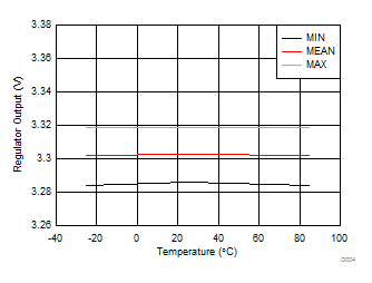
7.7 3.3-V Voltage Regulator
| PARAMETER | TEST CONDITION | MIN | TYP | MAX | UNIT | ||
|---|---|---|---|---|---|---|---|
| VCTL | Regulator control voltage (1)(2) | Measured at VCTL, V3P3 regulating | 3.3 | 26.4 | V | ||
| VV3P3 | Regulator output | Measured at V3P3, IREG = 0 to 4 mA, BAT = 4.2 to 26.4 V |
3.2 | 3.3 | 3.4 | V | |
| IREG | V3P3 output current | 4 | mA | ||||
| ISC | V3P3 short circuit current limit | V3P3 = 0.0 V | 10 | 17 | mA | ||
| VTB | Thermistor bias voltage | Measured at VTB, ITB = 0 | VV3P3 | V | |||
| ITB | Thermistor bias current | 1 | mA | ||||
| RTB | Thermistor bias internal resistance | RDS(ON) for internal FET switch, ITB = 1 mA | 90 | 130 | Ω | ||
(1) When a bypass FET is used to supply the regulated 3.3 V load current, VCTL automatically adjusts to keep V3P3 = 3.3 V. Note that VCTL,MIN and the FET VGS will determine the minimum BAT voltage at which the bypass FET will operate.
(2) If VCTL is tied to BAT, the load current is supplied through V3P3.
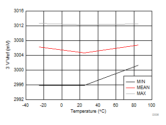
7.8 Voltage Reference
| PARAMETER | TEST CONDITION | MIN | TYP | MAX | UNIT | ||
|---|---|---|---|---|---|---|---|
| VREF | Voltage reference output | Before gain correction, TA = 25°C |
REF_SEL = 0 | 1.44 | 1.56 | V | |
| REF_SEL = 1 | 2.88 | 3.12 | |||||
| After gain correction, (1)
TA = 25°C |
REF_SEL = 0 | –0.1% | 1.5 | +0.1% | |||
| REF_SEL = 1 | –0.1% | 3 | +0.1% | ||||
| VREF_CAL | Reference calibration voltage | Measured at VCOUT | VCOUT_SEL = 2 | –0.9% | 0.5 × VREF | +0.9% | V |
| VCOUT_SEL = 3 | –0.5% | 0.85 × VREF | +0.5% | ||||
| (0.85 × VREF) – (0.5 × VREF) | –0.3% | 0.35 × VREF | +0.3% | V | |||
| ∆VREF | Voltage reference tolerance | TA = 0 – 50°C | –40 | 40 | ppm/°C | ||
| IREF | VREF output current | 10 | µA | ||||
(1) Gain correction factor determined at final test and stored in non-volatile storage. Gain correction is applied by Host controller.
7.9 Cell Voltage Amplifier
| PARAMETER | TEST CONDITION | MIN | TYP | MAX | UNIT | ||
|---|---|---|---|---|---|---|---|
| GVCOUT | Cell voltage amplifier gain | Measured from VCn to VCOUT |
REF_SEL = 0 | –1.6% | 0.3 | 1.5% | |
| REF_SEL = 1 | –1.6% | 0.6 | 1.5% | ||||
| OVCOUT | Cell voltage amplifier offset | Measured from VCn to VCOUT | –16 | 15 | mV | ||
| VCOUT | Cell voltage amp output range (1) | Measured at VCOUT, VCn = 5 V |
REF_SEL = 0 | 1.47 | 1.5 | 1.53 | V |
| REF_SEL = 1 | 2.94 | 3 | 3.06 | V | |||
| Measured at VCOUT, VCn = 0 V |
0 | V | |||||
| ∆VCOUT | Cell voltage amplifier accuracy | VCn = 1.4 V to 4.4 V, After correction, (2) Measured at VCOUT (3) REF_SEL = 1(4) |
TA = 25°C | –3 | 3 | mV | |
| TA = 0°C to 50°C | –5 | 5 | |||||
| TA = –25°C to +85°C | –8 | 8 | |||||
| IVCOUT | VCOUT output current(5) | 10 | µA | ||||
| tVCOUT | Delay from VCn select to VCOUT | Output step of 200 mV, COUT = 0.1 µF | 100 | µs | |||
(1) For VCn values greater than 5 V, VCOUT clamps at approximately V3P3.
(2) Correction factor determined at final test and stored in non-volatile storage. Correction is applied by Host controller.
(3) Output referred. Input referred accuracy is calculated as ∆VCOUT / GVCOUT (for example, 3 / 0.6 = 5).
(4) Correction factors are calibrated for gain of 0.6. Tolerance at gain of 0.3 is approximately doubled. Contact TI for information on devices calibrated to a gain of 0.3.
(5) Max DC load for specified accuracy.
7.10 Current Sense Amplifier
| PARAMETER | TEST CONDITION | MIN | TYP | MAX | UNIT | ||
|---|---|---|---|---|---|---|---|
| GVIOUT | Current sense amplifier gain | Measured from SENSEN, SENSEP to VIOUT |
I_GAIN = 0 | 4 | |||
| I_GAIN = 1 | 8 | ||||||
| VIIN | Current sense amp input range | Measured from SENSEN, SENSEP to VSS |
–125 | 375 | mV | ||
| VIOUT | Current sense amp output range | Measured at VIOUT | REF_SEL = 0 | 0.25 | 1.25 | V | |
| REF_SEL = 1 | 0.5 | 2.5 | V | ||||
| Zero current output | Measured at VIOUT SENSEP = SENSEN |
REF_SEL = 0 | 1 | V | |||
| REF_SEL = 1 | 2 | V | |||||
| ∆VIOUT | Current amplifier accuracy | –1% | 1% | ||||
| IVIOUT | VIOUT output current (1) | 10 | µA | ||||
(1) Max DC load for specified accuracy
7.11 Overcurrent Comparator
| PARAMETER | TEST CONDITION | MIN | TYP | MAX | UNIT | |
|---|---|---|---|---|---|---|
| VBAT_COMP | Minimum VBAT for comparator operation(1) | 5 | V | |||
| GVCOMP | Comparator amplifier gain | Measured from SENSEP to comparator input | 1 | |||
| VITRIP | Current comparator trip threshold(2) | 25 | 400 | mV | ||
| ∆VITRIP | Current comparator accuracy | VITRIP = 25 mV | –6 | 6 | mV | |
| VITRIP > 25 mV | –10% | 10% | V | |||
| VOL_ALERT | ALERT Output Low Logic | IALERT = 1 mA | 0.4 | V | ||
| VOH_ALERT | ALERT Output High Logic (3) | NA | NA | NA | ||
| IALERT | ALERT Pulldown current | ALERT = 0.4 V, Output driving low | 1 | mA | ||
| IALERT_LKG | ALERT Leakage current | ALERT = 5 V, Output Hi-Z | < 1 | μA | ||
| tOC | Comparator response time | 100 | µs | |||
(1) The Overcurrent Comparator is not guaranteed to work when VBAT is below this voltage.
(2) Trip threshold selectable from 25, 50, 75, 100, 125, 150, 175, 200, 225, 250, 275, 300, 325, 350, 375 or 400 mV.
(3) This parameter NA because output is open drain.
7.12 Internal Temperature Measurement
| PARAMETER | TEST CONDITION | MIN | TYP | MAX | UNIT | |
|---|---|---|---|---|---|---|
| VTEMP_INT | Internal temperature voltage | Measured at VCOUT, TINT = 25°C | 1.15 | 1.2 | 1.25 | V |
| ∆VTEMP_INT | Internal temperature voltage sensitivity | –4.4 | mV/°C | |||
7.13 Cell Balancing and Open Cell Detection
| PARAMETER | TEST CONDITION | MIN | TYP | MAX | UNIT | |
|---|---|---|---|---|---|---|
| RBAL | Cell balancing internal resistance(1) | RDS(ON) for VC1 internal FET switch, VCn = 3.6 V | 1 | 3 | 5 | Ω |
| RDS(ON) for internal VC2 to VC6 FET switch, VCn = 3.6 V | 3 | 5.5 | 8 | |||
(1) Balancing current is not internally limited. The cell balancing operation is completely controlled by the Host processor, no automatic function or time-out is included in the part. Take care to ensure that balancing current through the part is below the maximum power dissipation limit. The Host algorithm is responsible for limiting thermal dissipation to package ratings.
7.14 I2C Compatible Interface
| PARAMETERS | MIN | TYP | MAX | UNIT | ||
|---|---|---|---|---|---|---|
| DC PARAMETERS | ||||||
| VIL | Input Low Logic Threshold | 0.6 | V | |||
| VIH | Input High Logic Threshold | 2.8 | V | |||
| VOL | Output Low Logic Drive | IOL = 1 mA | 0.20 | V | ||
| IOL = 2.5 mA | 0.40 | |||||
| VOH | Output High Logic Drive (Not applicable due to open-drain outputs) | N/A | V | |||
| ILKG | I2C Pin Leakage | Pin = 5 V, Output in Hi-Z | < 1 | µA | ||
| AC PARAMETERS | ||||||
| tr | SCL, SDA Rise Time | 1000 | ns | |||
| tf | SCL, SDA Fall Time | 300 | ns | |||
| tw(H) | SCL Pulse Width High | 4 | µs | |||
| tw(L) | SCL Pulse Width Low | 4.7 | µs | |||
| tsu(STA) | Setup time for START condition | 4.7 | µs | |||
| th(STA) | START condition hold time after which first clock pulse is generated | 4 | µs | |||
| tsu(DAT) | Data setup time | 250 | ns | |||
| th(DAT) | Data hold time | 0(1) | µs | |||
| tsu(STOP) | Setup time for STOP condition | 4 | µs | |||
| tsu(BUF) | Time the bus must be free before new transmission can start | 4.7 | µs | |||
| t V | Clock Low to Data Out Valid | 900 | ns | |||
| th(CH) | Data Out Hold Time After Clock Low | 0 | ns | |||
| fSCL | Clock Frequency | 0 | 100 | kHz | ||
| tWAKE | I2C ready after transition to Wake Mode | 2.5 | ms | |||
(1) Devices must provide internal hold time of at least 300 ns for the SDA signal-to-bridge of the undefined region of the falling edge of SCL.
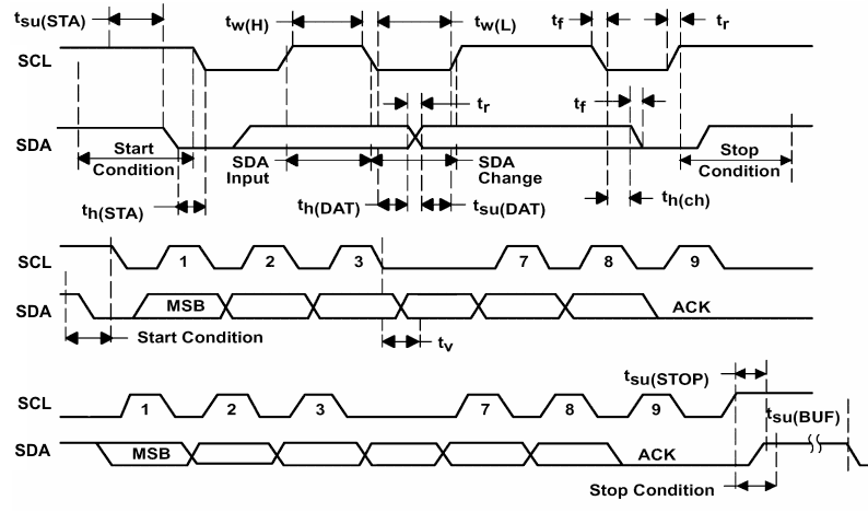 Figure 1. I2C Timing
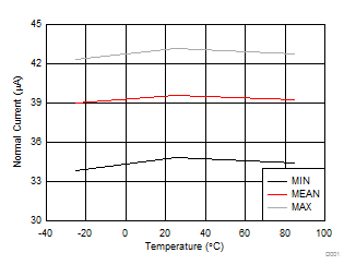
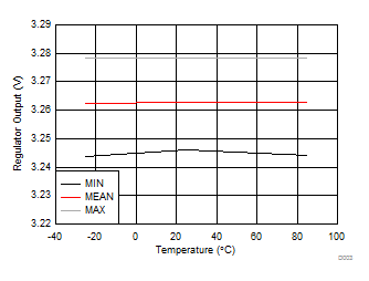
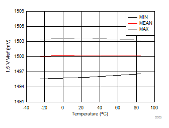
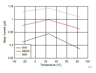
7.15 Typical Characteristics
