ZHCSED8 November 2015
PRODUCTION DATA.
6 Specifications
6.1 Absolute Maximum Ratings
Over operating free-air temperature range (unless otherwise noted)(1)| MIN | MAX | UNIT | ||
|---|---|---|---|---|
| Input voltage range, VIN | BAT, PACK (both under charge pump disabled condition) | –0.3 | 100 | V |
| CHG_EN, DSG_EN, PCHG_EN, PMON_EN, CP_EN(2) | –0.3 | 15 | V | |
| Output voltage range, VO | CHG, DSG, PCHG, PACKDIV, VDDCP | –0.3 | 100 | V |
| TFUNC | Functional Temperature | –40 | 110 | °C |
| Storage temperature, Tstg | –65 | 150 | °C | |
(1) Stresses beyond those listed under Absolute Maximum Ratings may cause permanent damage to the device. These are stress ratings only, which do not imply functional operation of the device at these or any other conditions beyond those indicated under Recommended Operating Conditions. Exposure to absolute-maximum-rated conditions for extended periods may affect device reliability.
(2) The enable inputs need to be current limited with max current not exceeding 5 mA.
6.2 ESD Ratings
| VALUE | UNIT | |||
|---|---|---|---|---|
| V(ESD) | Electrostatic discharge | Human-body model (HBM), per ANSI/ESDA/JEDEC JS-001(1) | ±2000 | V |
| Charged-device model (CDM), per JEDEC specification JESD22-C101(2) | ±500 | |||
(1) JEDEC document JEP155 states that 500-V HBM allows safe manufacturing with a standard ESD control process.
(2) JEDEC document JEP157 states that 250-V CDM allows safe manufacturing with a standard ESD control process.
6.3 Recommended Operating Conditions
Typical values stated where TA = 25°C and VBAT = 48.8 V, Min/Max values stated where TA = –40°C to 85°C and BAT = 8 V to 75 V (unless otherwise noted)| MIN | NOM | MAX | UNIT | ||||
|---|---|---|---|---|---|---|---|
| VBAT | Battery cell input supply voltage range | 8 | 75 | V | |||
| VPACK | Charger/Load voltage range | 0 | 75 | V | |||
| VIN | Input voltage range | CHG_EN, DSG_EN, PCHG_EN, PMON_EN, CP_EN | 0 | 14 | V | ||
| CVDDCP | Capacitor Between VDDCP and BAT | 470 | nF | ||||
| TOPR | Operating free-range temperature | –40 | 85 | °C | |||
6.4 Thermal Information
| THERMAL METRIC(1) | TSSOP (PW) | UNIT | |
|---|---|---|---|
| 16 PINS | |||
| RθJA, High K | Junction-to-ambient thermal resistance | 106.8 | °C/W |
| RθJC(top) | Junction-to-case(top) thermal resistance | 41.5 | °C/W |
| RθJB | Junction-to-board thermal resistance | 51.8 | °C/W |
| ψJT | Junction-to-top characterization parameter | 3.8 | °C/W |
| ψJB | Junction-to-board characterization parameter | 51.3 | °C/W |
| RθJC(bot) | Junction-to-case(bottom) thermal resistance | n/a | °C/W |
(1) For more information about traditional and new thermal metrics, see the Semiconductor and IC Package Thermal Metrics application report, SPRA953.
6.5 Electrical Characteristics
Typical values stated at TA = 25°C and V(BAT) = 48 V. MIN/MAX values stated with TA = –40°C to 85°C and V(BAT) = 8 to 75 V unless otherwise noted.| PARAMETER | DESCRIPTION | TEST CONDITION | MIN | TYP | MAX | UNIT |
|---|---|---|---|---|---|---|
| SUPPLY AND LEAKAGE CURRENT | ||||||
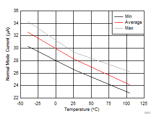
| I(BAT) | NORMAL mode current(1) | C(VDDCP) = 470 nF, V(BAT) = V(PACK), CL = 10 nF |
40 | 50 | µA | |
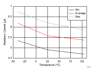
| Ishut | Sum of current into BAT and PACK pin | Shutdown Mode, PACK = 0 V, BAT = 8 V | 6 | 9.5 | µA | |
| CHARGE PUMP | ||||||
| V(VDDCP) | Charge pump voltage | No Load, CP_EN = hi, V(VDDCP) – V(BAT) | 9 | 14 | V | |
| tCPON | Charge pump start up time from zero volt | C(VDDCP) = 470 nF, 10% to 90% of V(VDDCP) | 100 | ms | ||
| INPUT ENABLE CONTROL SIGNALS | ||||||
| VIL | Digital low input level for CHG_EN, DSG_EN, PCHG_EN, CP_EN, PMON_EN | 0.6 | V | |||
| VIH | Digital high input level for CHG_EN, DSG_EN, PCHG_EN, CP_EN, PMON_EN | 1.2 | V | |||
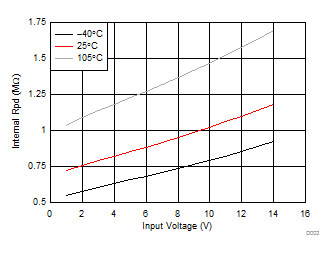
| RPD | Internal Pull down | VIN = 5 V | 0.6 | 1 | 4 | MΩ |
| CHARGE FET DRIVER | ||||||
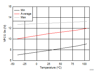
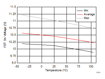
| V(CHGFETON) | CHG gate drive voltage (on) | CL = 10 nF, CHG_EN = Hi, V(BAT) = V(PACK), V(CHG) – V(BAT) | 9 | 12 | 14 | V |
| R(CHGFETON) | CHG FET driver on resistance | V(VDDCP) – V(BAT) = 12 V, CHG_EN = Hi, V(BAT) = V(PACK) | 1.1 | kΩ | ||
| R(CHGFETOFF) | CHG FET driver off resistance | V(VDDCP) – V(BAT) = 12 V, CHG_EN = Lo, V(BAT) = V(PACK) | 0.3 | kΩ | ||
| DISCHARGE FET DRIVER | ||||||
| V(DSGFETON) | DSG gate drive voltage (on) | CL = 10 nF, DSG_EN = Hi, V(BAT) = V(PACK), V(DSG) – V(PACK) | 9 | 12 | 14 | V |
| R(DSGFETON) | DSG FET driver on resistance | V(VDDCP) – V(BAT) = 12 V, DSG_EN = Hi, V(BAT) = V(PACK) | 3.5 | kΩ | ||
| R(DSGFETOFF) | DSG FET driver off resistance | V(VDDCP) – V(BAT) = 12 V, DSG_EN = Lo, V(BAT) = V(PACK) | 1 | kΩ | ||
| PRECHARGE FET DRIVER | ||||||
| V(PCHGFETON) | PCHG gate drive voltage (on) | V(PACK) > 17 V, V(BAT) < V(PACK), V(PACK) – V(PCHG) | 5 | 12 | 14 | V |
| PACK MONITOR (PACK_DIV) | ||||||
| R(PMONFET) | On resistance of internal FET (R between PACK and PACKDIV) | PMON_EN = hi | 1.5 | 2.5 | 3.5 | kΩ |
(1) NORMAL mode is defined as CHG_EN = Hi, DSG_EN = Hi, CP_EN = Hi, PCHG_EN = Lo, PMON_EN = Lo. Current value is averaged out over time.
6.6 Timing Requirements
| Parameter | Description | TEST CONDITION | MIN | TYP | MAX | UNIT |
|---|---|---|---|---|---|---|
| tCHGFETON | CHG on rise time + propagation delay | CL = 10 nF, (20% of CHG_EN from Lo to Hi) to (80% of V(CHGFETON)), CP_EN = Hi, (CP is already on) | 27 | 45 | µs | |
| tCHGFETOFF | CHG off fall time + progation delay | CL= 10 nF, (80% of CHG_EN from Hi to Lo) to (20% of V(CHGFETON)) , CHG_EN = Hi to Lo | 7 | 20 | µs | |
| tPROP _CHG | CHG EN to CHG output | CL= 10 nF, CP_EN = Hi, (CP is already on), see timing diagram | 0.5 | µs | ||
| tDSGFETON | DSG on rise time + propagation delay | CL = 10 nF, (20% of DSG_EN from Lo to Hi) to (80% of V(DSGFETON)), CP_EN = Hi, (CP is already on) | 24 | 50 | µs | |
| tDSGFETOFF | DSG off fall time + propagation delay | CL = 10 nF, (80% of DSG_EN from Hi to Lo) to (20% of V(DSGFETON)) | 7 | 20 | µs | |
| tPROP_DSG | DSG EN to DSG output propagation delay | CL= 10 nF, CP_EN = Hi, (CP already on), see timing Diagram | 0.5 | µs | ||
| tPCHGOFF | PCHG turn off time + propagation delay | CL = 1 nF, (20% of PCHG_EN from Hi to Lo) to (80% of V(PCHGFETON)) | 30 | 55 | µs | |
| tPCHGON | PCHG turn on time + propagation delay | CL = 1 nF, (80% of PCHG_EN from Lo to Hi) to (20% of V(PCHGFETON)) | 34 | 55 | µs | |
| tPROP_PCHG | PCH_EN to PCHG propagation delay | CL = 1 nF | 0.5 | µs | ||
| tPROP_PMON | PMON_EN and PACKDIV = PACK propagation delay | 0.5 | µs |
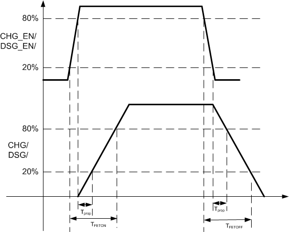 Figure 1. Timing Characteristics - ( CP assumed to be already On)
6.7 Typical Characteristics
