ZHCSED8 November 2015
PRODUCTION DATA.
8 Application and Implementation
NOTE
Information in the following applications sections is not part of the TI component specification, and TI does not warrant its accuracy or completeness. TI’s customers are responsible for determining suitability of components for their purposes. Customers should validate and test their design implementation to confirm system functionality.
8.1 Application Information
The bq76200 device is a high-side NMOS FET driver with integrated charge pump. The device can convert a low-side battery protection system into a high-side protection system, allowing the battery monitor device or battery MCU to always maintain communication to the host system regardless if the protection FETs are on or off. The device provides independent enables to control charge and discharge of a battery pack.
The following section highlights several recommended implementations when using this device. A detail bq76200 Application Note, SLVA729, is available at www.ti.com.
8.1.1 Recommended System Implementation
8.1.1.1 The bq76200 is a Slave Device
The bq76200 is a FET driver. It controls the output pins (CHG, DSG, PCHG, and PACKDIV) according to the input pin (CHG_EN, DSG_EN, PCHG_EN, CP_EN, and PMON_EN) status. The device does not validate if the inputs should or should not be turned on or off. For example, if both CHG_EN and PCHG_EN are enabled, bq76200 will turn on both CHG and PCHG simultaneously, enabling two charging paths to the system. The system designer should avoid undesirable enable combination via schematic, AFE, or host MCU implementation.
8.1.1.2 Flexible Control via AFE or via MCU
The bq76200 device has simple-logic input pins (CHG_EN, DSG_EN, PCHG_EN, CP_EN, and PMON_EN) that can accept a control signal from any MCU I/O. At the same time, the input pins are designed to tolerate high voltage signal such as the FET driver output from an AFE. This flexibility allows a mix of control input driving from AFE and/or MCU to optimize the system design.
For example, it is recommended to control the CP_EN pin via MCU which the system can turn on the charge pump at system start-up, excluding the extra FET delay due to charge pump voltage ramping. On the other hand, the CHG_EN and DSG_EN can be driven by the AFE FET driver output, especially if the AFE has hardware protection features (such as the bq76920/30/40 family), to optimize the FET reaction time.
All the input pins have internal pull-down resistor. The outputs are default to be off if any of the input pins are at high-Z state.
8.1.1.3 Scalable VDDCP Capacitor to Support Multiple FETs in Parallel
The bq76200 requires a minimum 470-nF capacitor to be connected between the VDDCP pin and BAT pin in order to turn on the integrated charge pump. The Electrical Characteristics Specification of this document specified the device performance based on 10 nF loading with 470-nF VDDCP capacitor. The loading capacitance varies with FET choices, number of FETs in use, and in parallel and simultaneous switching versus sequential switching of CHG and DSG FET.
The more FETs that are in parallel, the higher the loading capacitance. Similarly, simultaneously switching of the CHG and DSG FET loads down the charge pump more than sequentially switching both FETs. Eventually, the loading capacitance can exceed the supported range of a 470-nF VDDCP capacitor. A > 470-nF VDDCP capacitor can be used to support higher-loading capacitance.
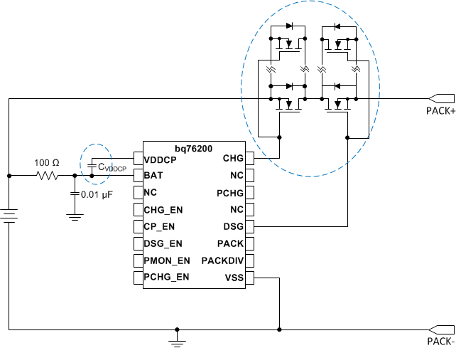 Figure 8. Scale CVDDCP to Support Multiple FETs in Parallel (Partial Schematic Shown)
Based on test results, 470-nF VDDCP capacitor can support up to approximately 30-nF loading capacitance. Using a 470-nF/20-nF ratio (to include some design margin), a 2.1-µF VCCDP capacitor can support up to ~90 nF loading capacitance. Note that a larger VDDCP capacitor increases the charge pump start up time; a higher loading capacitance increases the FET on and off time. System designers should test across the operation range to ensure the design margin and system performance. Refer to the bq76200 Application note for more test results.
Also notice that any damage or disconnection of the VDDCP capacitor during operation can leave a residual voltage on the FET driver output if the inputs are enabled. This can result in putting the external FETs in a high-Rdson state and cause FET damage.
8.1.1.4 Pre-Charge and Pre-Discharge Support
For a deeply depleted battery pack, a much lower charging current, for example, a C/10 rate, is usually used to pre-charge the battery cells. This allows the passivating layer of the cell to be recovered slowly (the passivating layer might be dissolved in the deep discharge state).
The bq76200 has a PCHG output to drive an external P-channel FET to support battery pre-charge. In this scenario, the external P-channel FET is placed in parallel with the CHG FET and a power resistor can be connected in series of the P-channel FET to limit the charging current during the pre-charge state. The MCU can be used to control the PCHG_EN pin to determine the entry and exit of the pre-charge mode.
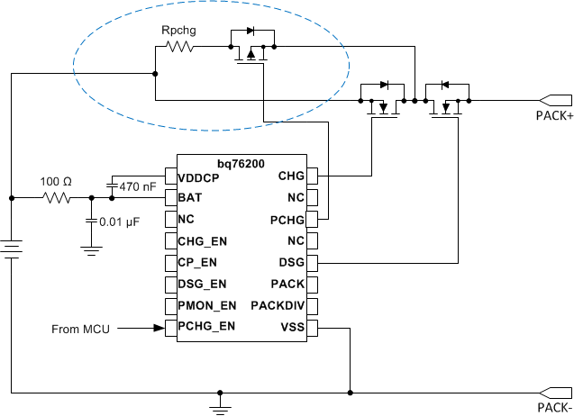 Figure 9. P-channel FET in Parallel With CHG FET for Pre-Charging (Partial Schematic Shown)
Alternatively, the CHG pin can also be used to pre-charge a battery pack given if the charging current is controlled by the system (i.e. does not require external component to limit the charging current such as a smart charger) and the battery stack voltage is higher than minimum operation voltage of the bq76200 (i.e. the charge pump can start to turn on the CHG FET). PCHG should leave floating if it is not used in the application.
The PCHG output can be used to pre-discharge a high-capacitive system. For example, a load removal can be one of the recovery requirements after a discharge related fault has been detected. In a high-capacitive system, the residual voltage at the system side can take a significant time to bleed off. This results in an additional delay in fault recovery. The PCHG output can be used to control an external P-channel FET placed in parallel with the DSG FET to pre-discharge the residual voltage in order to speed up the fault recovery process.
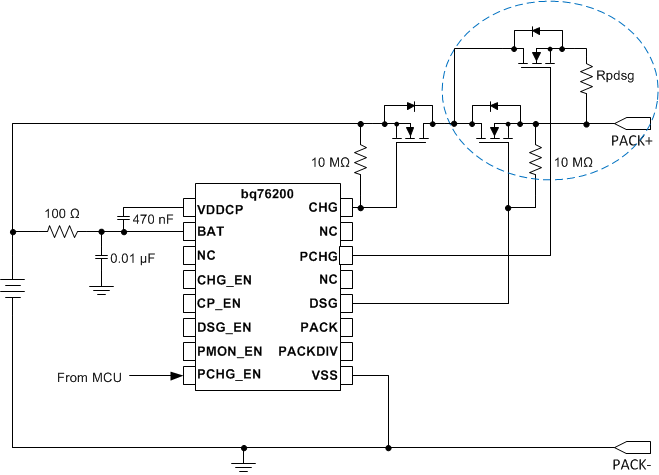 Figure 10. P-channel FET in Parallel with DSG FET for Pre-Discharging (Partial Schematic Shown)
8.1.1.5 Optional External Gate Resistor
The CHG and DSG have certain internal on and off resistance. However, an optional external gate resistor can be added to CHG and/or DSG FET to slow down the FET on and off timing.
8.1.1.6 Separate Charge and Discharge paths
In some systems, the charging current might be significantly lower than the discharge current. In such systems, the system designer may prefer to implement a separate charge and discharge paths in which the number of FET in parallel for charge and discharge can be different to reduce to BOM cost.
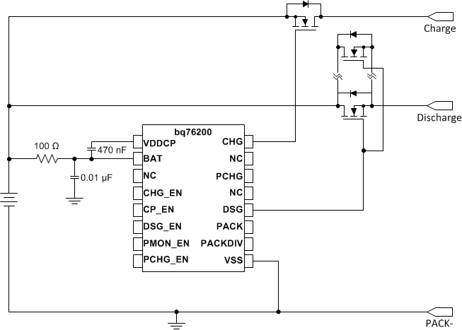 Figure 11. Separate Charge and Discharge Paths (Partial Schematic Shown)
8.2 Typical Applications
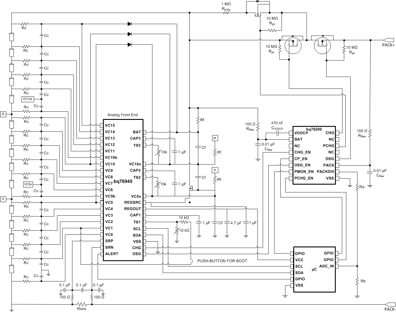
8.2.1 Design Requirements
For this design example, use the parameters listed in Table 2.
Table 2. Design Parameters
8.2.2 Detailed Design Procedure
- Determine if CP_EN pin will be driven by MCU. It is highly recommended to use CP_EN to turn on the charge pump at system start-up. However, it is not a must to operate the bq76200 to switch on CHG and DSG pins. System designer should ensure the FET's turn on time is acceptable during normal operation if CP_EN is not enabled at system startup.
- Select the correct VDDCP capacitance. Scaling up the VDDCP capacitance allows support for a higher number of FETs in parallel. This test result of various parallel FETs versus VDDCP capacitance in the bq76200 application is for general reference only. System designer should always validate their design tolerant across operation temperature range.
- If the PMON_EN is used, the PACKDIV resistor divider, Ra and Rb, must be selected to satisfy (Ra+Rb) < 500uA, AND [Rb/(Ra + Rb)] < (max ADC input range)/(max PACK+ voltage). For example, In a 48V system, if the max charger voltage is 50.4V and a MCU's max ADC input is 3V. To meet both (Ra + Rb) < 500uA, AND [Rb/(Ra + Rb)] < (3V/50.4V) requirements, the Ra value might be 100 kΩ or less and Rb value might be 6 KΩ or less.
- Follow the application schematic (see Typical Applications) to connect the device.
8.2.3 Application Curves
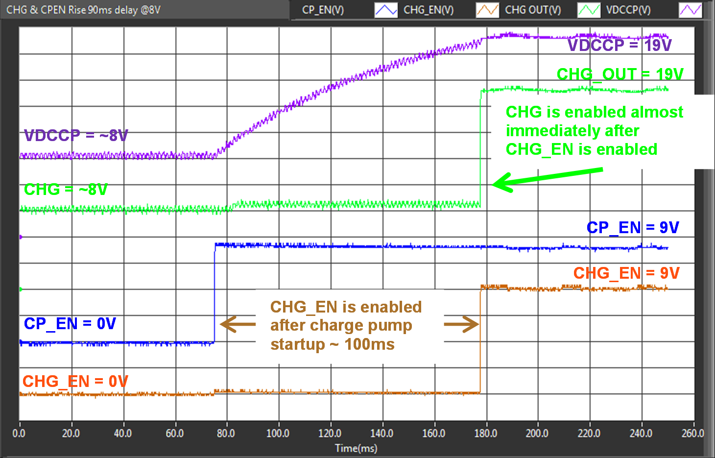
| CHG output reacts to the CHG_EN signal immediately. Similar behavior applies to DSG pin. |
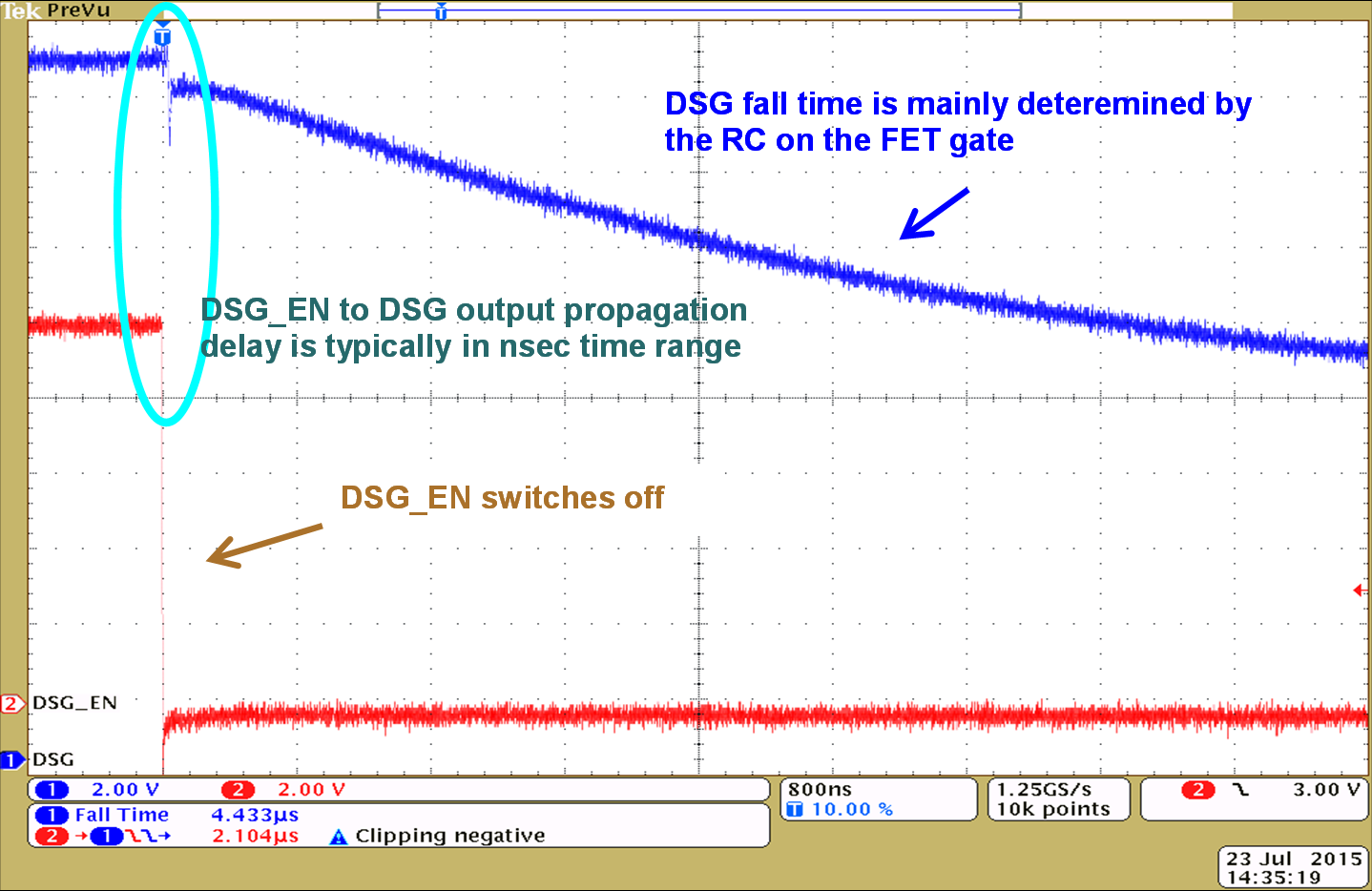
| With 10 nF loading and no Rgs on DSG output. Note the time scale was 800ns/div. Hence, the DSG waveform above was basically the DSG FET fall time | ||
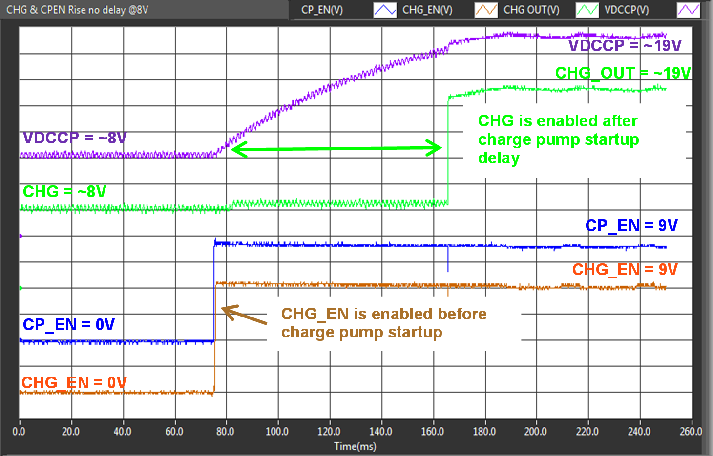
| CHG output reacts to the CHG_EN signal after charge pump startup delay. Similar behavior applies to DSG pin. |