ZHCSGA3A march 2017 – march 2023 BQ25601
PRODUCTION DATA
- 1 特性
- 2 应用
- 3 说明
- 4 Revision History
- 5 说明(续)
- 6 Device Comparison Table
- 7 Pin Configuration and Functions
- 8 Specifications
-
9 Detailed Description
- 9.1 Overview
- 9.2 Functional Block Diagram
- 9.3
Feature Description
- 9.3.1 Power-On-Reset (POR)
- 9.3.2 Device Power Up from Battery without Input Source
- 9.3.3 Power Up from Input Source
- 9.3.4 Boost Mode Operation From Battery
- 9.3.5 Host Mode and Standalone Power Management
- 9.3.6 Power Path Management
- 9.3.7 Battery Charging Management
- 9.3.8 Protections
- 9.4 Device Functional Modes
- 9.5 Programming
- 9.6 Register Maps
- 10Application and Implementation
- 11Power Supply Recommendations
- 12Layout
- 13Device and Documentation Support
- 14Mechanical, Packaging, and Orderable Information
7 Pin Configuration and Functions
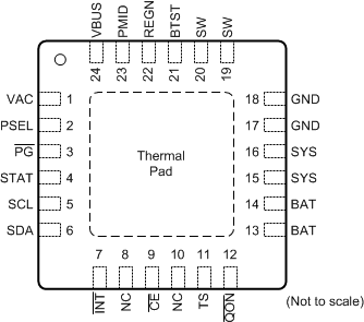
 Figure 7-1 RTW Package24-Pin WQFNTop View
Table 7-1 Pin Functions
| PIN | TYPE(1) | DESCRIPTION | |
|---|---|---|---|
| NAME | NO. | ||
| BAT | 13 | P | Battery connection point to the positive terminal of the battery pack. The internal BATFET and current sensing is connected between SYS and BAT. Connect a 10 µF close to the BAT pin. |
| 14 | |||
| BTST | 21 | P | PWM high side driver positive supply. Internally, the BTST pin is connected to the cathode of the boost-strap diode. Connect the 0.047-μF bootstrap capacitor from SW to BTST. |
| CE | 9 | DI | Charge enable pin. When this pin is driven low, battery charging is enabled. |
| GND | 17 | P | Ground. |
| 18 | |||
| INT | 7 | DO | Open-drain interrupt Output. Connect the INT to a logic rail through 10-kΩ resistor. The INT pin sends an active low, 256-µs pulse to host to report charger device status and fault. |
| NC | 8 | — | No Connect. Keep the pins float. |
| 10 | |||
| PG | 3 | DO | Open drain active low power good indicator. Connect to the pull up rail through 10-kΩ resistor. LOW indicates a good input source if the input voltage is between UVLO and ACOV, above SLEEP mode threshold, and current limit is above 30 mA. |
| PMID | 23 | DO | Connected to the drain of the reverse blocking MOSFET (RBFET) and the drain of HSFET. Put 10 μF ceramic capacitor on PMID to GND. |
| PSEL | 2 | DI | Power source selection input. Set 500 mA input current limit by pulling this pin high and set 2.4A input current limit by pulling this pin low. Once the device gets into host mode, the host can program different input current limits to IINDPM register. |
| QON | 12 | DI | BATFET enable/reset control input. When BATFET is in ship mode, a logic low of tSHIPMODE duration turns on BATFET to exit shipping mode. When VBUS is not plugged in, a logic low of tQON_RST (minimum 8 s) duration resets SYS (system power) by turning BATFET off for tBATFET_RST (minimum 250 ms) and then re-enable BATFET to provide full system power reset. The pin contains an internal 200-kΩ pull-up to maintain default high logic. |
| REGN | 22 | P | LSFET driver and internal supply output. Internally, REGN is connected to the anode of the boost-strap diode. Connect a 4.7-μF (10-V rating) ceramic capacitor from REGN to GND. The capacitor should be placed close to the IC. |
| SCL | 5 | DI | I2C interface clock. Connect SCL to the logic rail through a 10-kΩ resistor. |
| SDA | 6 | DIO | I2C interface data. Connect SDA to the logic rail through a 10-kΩ resistor. |
| STAT | 4 | DO | Open-drain charge status output. Connect the STAT pin to a logic
rail via 10-kΩ resistor. The STAT pin indicates charger status.
Collect a current limit resister and a LED from a rail to this pin.
Charge in progress: LOW Charge complete or charger in SLEEP mode: HIGH Charge suspend (fault response): 1-Hz, 50% duty cycle Pulses This pin can be disabled via EN_ICHG_MON[1:0] register bits. |
| SW | 19 | P | Switching node output. Connected to output inductor. Connect the 0.047-μF bootstrap capacitor from SW to BTST. |
| 20 | |||
| SYS | 15 | P | Converter output connection point. The internal current sensing network is connected between SYS and BAT. Connect a 20 µF capacitor close to the SYS pin. |
| 16 | |||
| TS | 11 | AI | Temperature qualification voltage input to support JEITA profile. Connect a negative temperature coefficient thermistor. Program temperature window with a resistor divider from REGN to TS to GND. Charge suspends when TS pin is out of range. When TS pin is not used, connect a 10-kΩ resistor from REGN to TS and connect a 10-kΩ resistor from TS to GND. It is recommended to use a 103AT-2 thermistor. |
| VAC | 1 | AI | Charge input voltage sense. This pin must be connected to VBUS pin. |
| VBUS | 24 | P | Charger input. The internal n-channel reverse block MOSFET (RBFET) is connected between VBUS and PMID pins. Place a 1-uF ceramic capacitor from VBUS to GND close to device. |
| Thermal Pad | — | P | Thermal pad and ground reference. This pad is ground reference for the device and it is also the thermal pad used to conduct heat from the device. This pad should be tied externally to a ground plane through PCB vias under the pad. |
(1) AI = Analog input, AO = Analog Output, AIO = Analog input
Output, DI = Digital input, DO = Digital Output, DIO = Digital input Output, P =
Power