ZHCSBN3F August   2013  – March 2019

PRODUCTION DATA.  

  1. 特性
  2. 应用
  3. 说明
    1.     Device Images
      1.      简化原理图
      2.      充电器效率
  4. 修订历史记录
  5. Pin Configuration and Functions
    1.     Pin Functions
  6. Specifications
    1. 6.1 Absolute Maximum Ratings
    2. 6.2 ESD Ratings
    3. 6.3 Recommended Operating Conditions
    4. 6.4 Thermal Information
    5. 6.5 Electrical Characteristics
    6. 6.6 Typical Characteristics
  7. Detailed Description
    1. 7.1 Overview
    2. 7.2 Functional Block Diagram
    3. 7.3 Feature Description
      1. 7.3.1 Maximum Power Point Tracking
      2. 7.3.2 Battery Undervoltage Protection
      3. 7.3.3 Battery Overvoltage Protection
      4. 7.3.4 Battery Voltage in Operating Range (VBAT_OK Output)
      5. 7.3.5 Push-Pull Multiplexer Drivers
      6. 7.3.6 Nano-Power Management and Efficiency
    4. 7.4 Device Functional Modes
      1. 7.4.1 Main Boost Charger Disabled (Ship Mode) - (VSTOR > VSTOR_CHGEN and EN = HIGH)
      2. 7.4.2 Cold-Start Operation (VSTOR < VSTOR_CHGEN, VIN_DC > VIN(CS) and PIN > PIN(CS))
      3. 7.4.3 Main Boost Charger Enabled (VSTOR > VSTOR_CHGEN, VIN_DC > VIN(DC) and EN = LOW )
      4. 7.4.4 Thermal Shutdown
  8. Application and Implementation
    1. 8.1 Application Information
      1. 8.1.1 Energy Harvester Selection
      2. 8.1.2 Storage Element Selection
      3. 8.1.3 Inductor Selection
      4. 8.1.4 Capacitor Selection
        1. 8.1.4.1 VREF_SAMP Capacitance
        2. 8.1.4.2 VIN_DC Capacitance
        3. 8.1.4.3 VSTOR Capacitance
        4. 8.1.4.4 Additional Capacitance on VSTOR or VBAT_SEC
    2. 8.2 Typical Applications
      1. 8.2.1 Solar Application Circuit
        1. 8.2.1.1 Design Requirements
        2. 8.2.1.2 Detailed Design Procedure
        3. 8.2.1.3 Application Performance Plots
      2. 8.2.2 TEG Application Circuit
      3. 8.2.3 Design Requirements
        1. 8.2.3.1 Detailed Design Procedure
        2. 8.2.3.2 Application Performance Plots
      4. 8.2.4 Piezoelectric Application Circuit
        1. 8.2.4.1 Design Requirements
        2. 8.2.4.2 Detailed Design Procedure
        3. 8.2.4.3 Application Curves
  9. Power Supply Recommendations
  10. 10Layout
    1. 10.1 Layout Guidelines
    2. 10.2 Layout Example
    3. 10.3 Thermal Considerations
  11. 11器件和文档支持
    1. 11.1 器件支持
      1. 11.1.1 第三方产品免责声明
      2. 11.1.2 Zip 文件
    2. 11.2 文档支持
      1. 11.2.1 相关文档
    3. 11.3 接收文档更新通知
    4. 11.4 社区资源
    5. 11.5 商标
    6. 11.6 静电放电警告
    7. 11.7 术语表
  12. 12机械、封装和可订购信息

封装选项

机械数据 (封装 | 引脚)
散热焊盘机械数据 (封装 | 引脚)
订购信息

Application Performance Plots

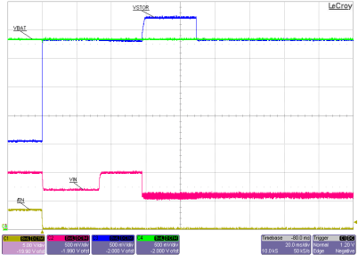
bq25505 bq25570-EN-TOG-VOUT-EN_GND_lusbh2.gif
VIN_DC = 1.0 V power supply 100Ω series resistance
VBAT = 3.4-V charged Li coin cell
Figure 29. Startup by Taking EN Low (From Ship Mode)
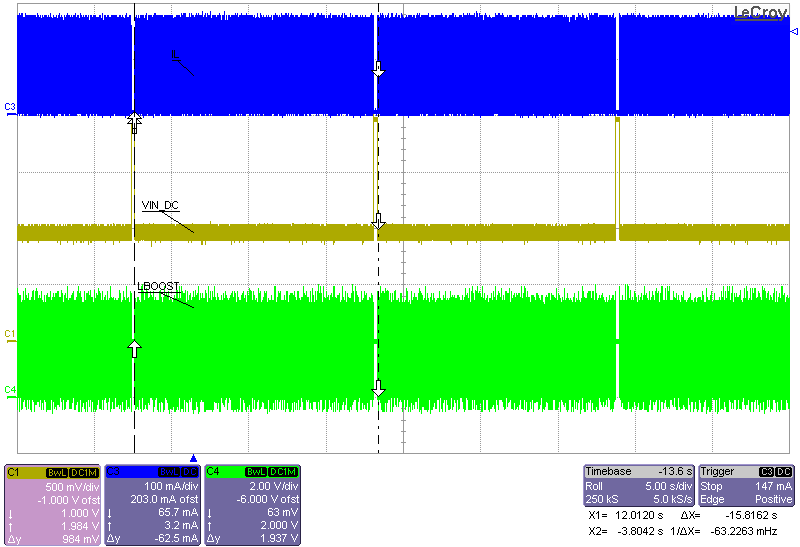
bq25505 mppt_ov_5p0v_3vstor_2p0vin_42p6ma_slusbj3.png
VIN_DC = sourcemeter with VSOURCE = 2.0 V and compliance of 43 mA
VBAT_SEC = sourcemeter with VSOURCE = 3.0 V and compliance of 1 A
Figure 31. MPPT Operation
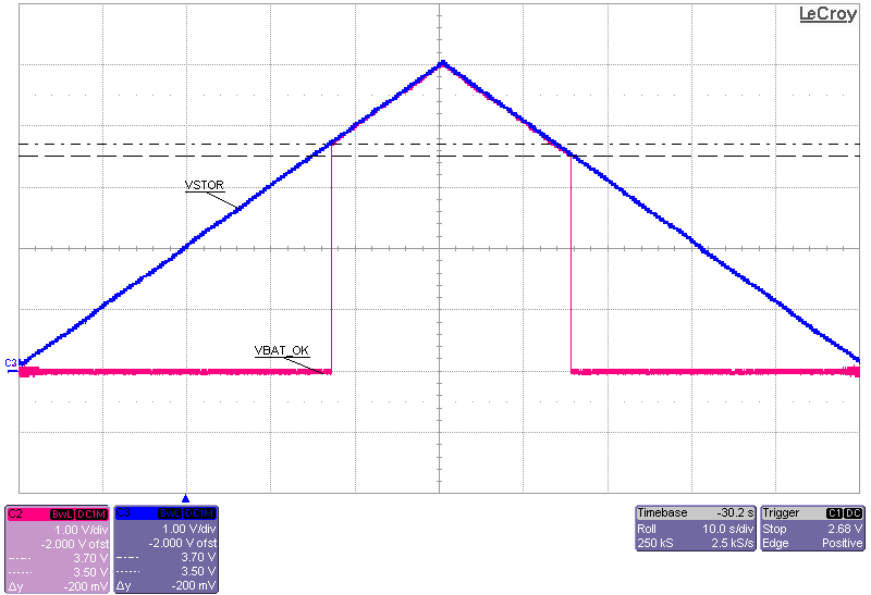
bq25505 app2_ov_5p0v_Vbatok_slusbj3.png
VIN_DC floating
No storage element on VBAT or VBAT_PRI
VSTOR artifically ramped from 0 V to 5 V to 0 V using a function generator
Figure 33. VBAT_OK Operation
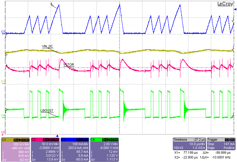
bq25505 app2_operation_ov_5p0v_3vstor_2p0vin_42p6ma_slusbj3.png
VIN_DC = sourcemeter with VSOURCE = 2.0 V and compliance of 43 mA
VBAT_SEC = sourcemeter with VSOURCE = 3.0 V and compliance of 1 A
Figure 30. Boost Charger Operational Waveforms
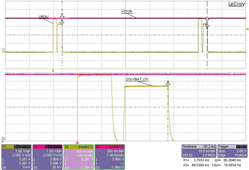
bq25505 app2_ov_5v_VRDIV1_slusbj3.png
VIN_DC = sourcemeter with VSOURCE = 2.0 V and compliance of 43 mA
VBAT_SEC = sourcemeter with VSOURCE = 4.0 V and compliance of 1 A
Figure 32. VRDIV Waveform