ZHCSEY1 April 2016
PRODUCTION DATA.
- 1 特性
- 2 应用
- 3 说明
- 4 修订历史记录
- 5 Device Comparison Table
- 6 Pin Configuration and Functions
- 7 Specifications
- 8 Detailed Description
- 9 Application and Implementation
- 10Power Supply Recommendations
- 11Layout
- 12器件和文档支持
- 13机械、封装和可订购信息
8 Detailed Description
8.1 Overview
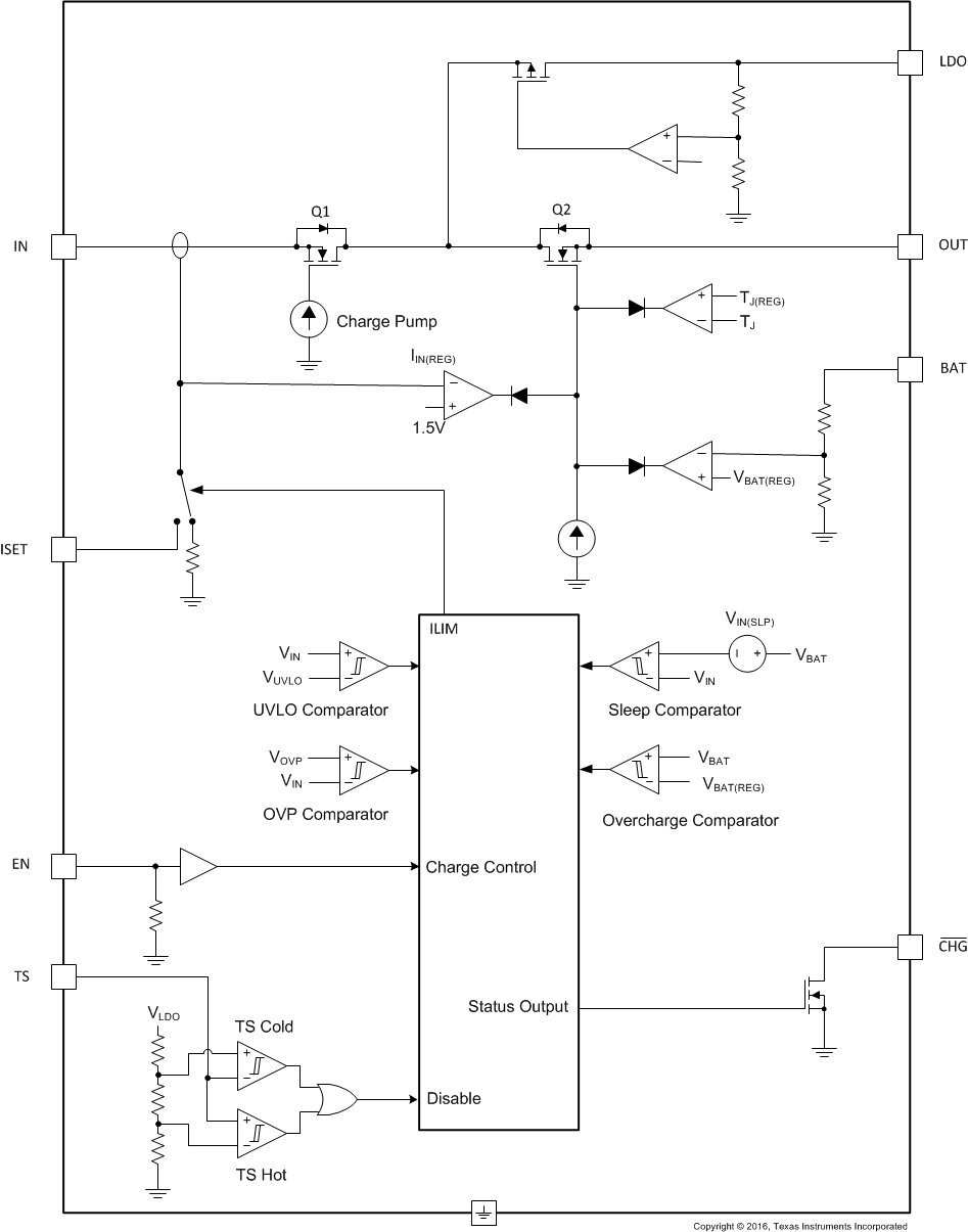
The bq25071-Q1 is a highly integrated, automotive qualified, linear, LiFePO4 battery charger targeted at space-limited automotive applications. It accepts power from either a USB port or AC adapter and charges a single-cell LiFePO4 battery with up to 1 A of charge current. The 30 V input rating with 10.5 V input overvoltage protection supports low-cost unregulated adapters.
The bq25071-Q1 has a single power output that simultaneously charges the battery and powers the system. The input current is programmable from 100 mA up to 1 A using the ISET input or configurable for USB500. There is also a 4.9 V ±10% 50 mA LDO is integrated into the IC for supplying low power external circuitry.
The LiFePO4 charging algorithm removes the constant voltage mode control typically used in Li-Ion battery charge cycles which reduces charge time significantly. Instead, the battery is fast charged to the overcharge voltage and then allowed to relax to a lower float charge voltage threshold. The charger power stage and charge current sense functions are fully integrated. The charger function has high accuracy current and voltage regulation loops, and charge status display. During the charge cycle, an internal control loop monitors the IC junction temperature and reduces the charge current if an internal temperature threshold is exceeded.
8.2 Functional Block Diagram

8.3 Feature Description
8.3.1 Input Overvoltage Protection
The bq25071-Q1 contains an input overvoltage protection circuit that disables the LDO output and charging when the input voltage rises above V(OVP). This prevents damage from faulty adapters. The OVP circuitry contains an 100 μs blanking period that prevents ringing on the input from line transients from tripping the OVP circuitry falsely. If an adapter with an output greater than V(OVP) is plugged in, the IC completes soft-start power up and then shuts down if the voltage remains above V(OVP) after 100 μs. The LDO remains off and charging remains disabled until the input voltage falls below V(OVP).
8.3.2 Undervoltage Lockout (UVLO)
The bq25071-Q1 remains in power down mode when the input voltage is below the undervoltage lockout threshold (V(UVLO)). During this mode, the control input (EN) is ignored. The LDO, the charge FET connected between IN and OUT are off and the status output (CHG) is high impedance. Once the input voltage rises above V(UVLO), the internal circuitry is turned on and the normal operating procedures are followed.
8.3.3 External NTC Monitoring (TS)
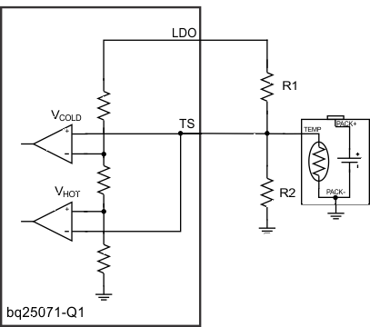
The bq25071-Q1 features a flexible, voltage based external battery pack temperature monitoring input. The TS input connects to the NTC thermistor in the battery pack to monitor battery temperature and prevent dangerous over-temperature conditions. During charging, the voltage at TS is continuously monitored. If the voltage at the TS pin is outside of the operating range (V(HOT) to V(COLD) for longer than the built in 25 ms deglitch time, charging is suspended. When the voltage measured at TS returns to within the operation window, charging resumes. When a battery pack temperature fault occurs charging is suspended, but the CHG output remains low and continues to indicate charging.
The temperature thresholds are programmed using a resistor divider from LDO to GND with the NTC thermistor connected to the center tap from TS to GND. See Figure 9 for the circuit example. The value of R1 and R2 are calculated using the following equations:


RHOT is the expected thermistor resistance at the programmed hot threshold; RCOLD is the expected thermistor resistance at the programmed cold threshold.

8.3.4 50-mA LDO (LDO)
The LDO output of the bq25071-Q1 is a low dropout linear regulator (LDO) that supplies up to 50 mA while regulating to V(LDO). The LDO is active whenever the input voltage is above V(UVLO) and below V(OVP). It is not affected by the EN input. The LDO output is used to power and protect circuitry such as USB transceivers from transients on the input supply.
8.3.5 Charge Status Indicator (CHG)
The bq25071-Q1 contains an open drain CHG output that indicates charging state and faults. When charging a battery in precharge or fastcharge mode, the CHG output is pulled to GND. Once the BAT output reaches the overcharge voltage threshold, CHG goes high impedance to signal the battery is fully charged. When the battery voltage drops below the recharge voltage threshold the CHG output is pulled low to signal the host of a new charge cycle. Connect CHG to the required logic level voltage through a 1 kΩ to 100 kΩ resistor to use the signal with a microprocessor. I(CHG) must be below 5 mA.
The IC monitors the CHG pin when no input is connected to verify if the system circuitry is active. If the voltage at CHG is logic being drive low when no input is connected, the TS circuit is turned off for a low quiescent current state. Once the voltage at CHG increases above logic high, the TS circuit is turned on.
8.3.6 Input Current Limit Control (EN)
The bq25071-Q1 contains a 3-state that controls the input current limit. Drive EN low to program the input current limit to the user defined value programmed using ISET. Drive EN high to place the bq25071-Q1 in USB suspend mode. In USB suspend mode, the input current into bq25071-Q1 is reduced. Leaving EN unconnected or connected to a high impedance source programs the USB500 input current limit.
Table 1. EN Input Definition
| EN | MODE |
|---|---|
| Low | ISET |
| Hi-Z | USB500 |
| Hi | USB Suspend |
8.4 Device Functional Modes
8.4.1 Charging Operation
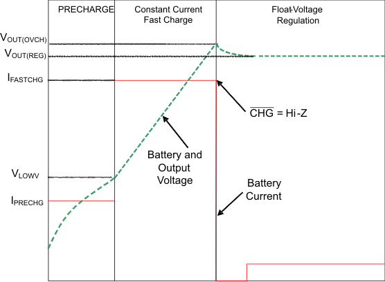
The bq25071-Q1 uses a charge algorithm that is unique to LiFePO4 chemistry cells. The current taper typically seen as part of the constant voltage mode control usually present in Li-Ion battery charge cycles is replaced with a floating regulation voltage with minimal charging current. This dramatically decreases the charge time. When the bq25071-Q1 is enabled by EN, the battery voltage is monitored to verify which stage of charging must be used. When V(BAT) < V(LOWV), the bq25071-Q1 charges in precharge mode; when V(BAT) > V(LOWV), the normal charge cycle is used.
8.4.1.1 Charger Operation with Minimum System Voltage Mode Enabled
 Figure 10. Typical Charging Cycle with Minimum System Voltage Enabled
8.4.1.2 Precharge Mode (V(BAT) ≤ V(LOWV))
The bq25071-Q1 enters precharge mode when VBAT ≤ V(LOWV). Upon entering precharge mode, the battery is charged with a 47.5 mA current and CHG goes low.
8.4.1.3 Fast Charge Mode
Once V(BAT) > V(LOWV), the bq25071-Q1 enters constant current (CC) mode where charge current is regulated using the internal MOSFETs between IN and OUT. The total current is shared between the output load and the battery. Once the battery voltage charges up to VBAT(OVCH), the CHG output goes high indicating the charge cycle is complete and the bq25071-Q1 switches the battery regulation voltage to VBAT(REG). The battery voltage is allowed to relax down to VBAT(REG). The charger remains enabled and regulates the output to VBAT(REG). If at any time the battery falls below V(RCH), the charge cycle restarts.
8.4.2 Programmable Input Current Limit (ISET)
When the charger is enabled, and the user programmable current limit is selected by the EN input, internal circuits generate a current proportional to the input current at the ISET input. The current out of ISET is 1/1000 (±10%) of the charge current. This current, when applied to the external charge current programming resistor, R1 ( Figure 11), generates an analog voltage that is regulated to program the fast charge current. Connect a resistor from ISET to GND to program the input current limit using the following equation:

I(IN_LIM) is programmable from 100 mA to 1 A. The voltage at ISET can be monitored by an external host to calculate the charging current to the battery. The input current is related to the ISET voltage using the following equation:

Monitoring the ISET voltage allows for the host to calculate the actual charging current and therefore perform more accurate termination. The input current to the system must be monitored and subtracted from the current into the bq25071-Q1 which is show by V(ISET).
8.4.3 Sleep Mode
If the IN pin voltage is between V(UVLO) and V(BAT)+ VIN(SLP), the charge current is disabled, the safety timer counting stops (not reset) and the CHG pin is high impedance. As the input voltage rises and the charger exits sleep mode, the safety timer continues to count, charge is enabled and the CHG pin returns to its previous state.
8.4.4 Thermal Regulation and Thermal Shutdown
The bq25071-Q1 contains a thermal regulation loop that monitors the die temperature continuously. If the temperature exceeds TJ(REG), the device automatically reduces the charging current to prevent the die temperature from increasing further. In some cases, the die temperature continues to rise despite the operation of the thermal loop, particularly under high VIN conditions. If the die temperature increases to TJ(OFF), the IC is turned off. Once the device die temperature cools by TJ(OFF-HYS), the device turns on and returns to thermal regulation. Continuous overtemperature conditions result in the pulsing of the load current. If the junction temperature of the device exceeds TJ(OFF), the charge FET is turned off. The FET is turned back on when the junction temperature falls below TJ(OFF) – TJ(OFF-HYS).
Note that these features monitor the die temperature of the bq25071-Q1. This is not synonymous with ambient temperature. Self heating exists due to the power dissipated in the IC because of the linear nature of the battery charging algorithm.