ZHCSFE1B June   2016  – August 2017 ADS8920B , ADS8922B , ADS8924B

PRODUCTION DATA.  

  1. 特性
  2. 应用
  3. 说明
    1.     Device Images
      1.      使用 ADS89xxB 集成功能轻松实现 系统设计
  4. Revision History
  5. Pin Configuration and Functions
    1.     Pin Functions
  6. Specifications
    1. 6.1 Absolute Maximum Ratings
    2. 6.2 ESD Ratings
    3. 6.3 Recommended Operating Conditions
    4. 6.4 Thermal Information
    5. 6.5 Electrical Characteristics
    6. 6.6 Timing Requirements
    7. 6.7 Switching Characteristics
    8. 6.8 Typical Characteristics
  7. Detailed Description
    1. 7.1 Overview
    2. 7.2 Functional Block Diagram
    3. 7.3 Feature Description
      1. 7.3.1 LDO Module
      2. 7.3.2 Reference Buffer Module
      3. 7.3.3 Converter Module
        1. 7.3.3.1 Sample-and-Hold Circuit
        2. 7.3.3.2 Internal Oscillator
        3. 7.3.3.3 ADC Transfer Function
      4. 7.3.4 Interface Module
    4. 7.4 Device Functional Modes
      1. 7.4.1 RST State
      2. 7.4.2 ACQ State
      3. 7.4.3 CNV State
    5. 7.5 Programming
      1. 7.5.1 Output Data Word
      2. 7.5.2 Data Transfer Frame
      3. 7.5.3 Interleaving Conversion Cycles and Data Transfer Frames
      4. 7.5.4 Data Transfer Protocols
        1. 7.5.4.1 Protocols for Configuring the Device
        2. 7.5.4.2 Protocols for Reading From the Device
          1. 7.5.4.2.1 Legacy, SPI-Compatible (SYS-xy-S) Protocols
          2. 7.5.4.2.2 SPI-Compatible Protocols with Bus Width Options
          3. 7.5.4.2.3 Source-Synchronous (SRC) Protocols
            1. 7.5.4.2.3.1 Output Clock Source Options with SRC Protocols
            2. 7.5.4.2.3.2 Bus Width Options With SRC Protocols
            3. 7.5.4.2.3.3 Output Data Rate Options With SRC Protocols
      5. 7.5.5 Device Setup
        1. 7.5.5.1 Single Device: All multiSPI Options
        2. 7.5.5.2 Single Device: Minimum Pins for a Standard SPI Interface
        3. 7.5.5.3 Multiple Devices: Daisy-Chain Topology
        4. 7.5.5.4 Multiple Devices: Star Topology
    6. 7.6 Register Maps
      1. 7.6.1 Device Configuration and Register Maps
        1. 7.6.1.1 PD_CNTL Register (address = 04h) [reset = 00h]
          1. Table 11. PD_CNTL Register Field Descriptions
        2. 7.6.1.2 SDI_CNTL Register (address = 008h) [reset = 00h]
          1. Table 12. SDI_CNTL Register Field Descriptions
        3. 7.6.1.3 SDO_CNTL Register (address = 0Ch) [reset = 00h]
          1. Table 13. SDO_CNTL Register Field Descriptions
        4. 7.6.1.4 DATA_CNTL Register (address = 010h) [reset = 00h]
          1. Table 14. DATA_CNTL Register Field Descriptions
        5. 7.6.1.5 PATN_LSB Register (address = 014h) [reset = 00h]
          1. Table 15. PATN_LSB Register Field Descriptions
        6. 7.6.1.6 PATN_MID Register (address = 015h) [reset = 00h]
          1. Table 16. PATN_MID Register Field Descriptions
        7. 7.6.1.7 PATN_MSB Register (address = 016h) [reset = 00h]
          1. Table 17. PATN_MSB Register Field Descriptions
        8. 7.6.1.8 OFST_CAL Register (address = 020h) [reset = 00h]
          1. Table 18. OFST_CAL Register Field Descriptions
        9. 7.6.1.9 REF_MRG Register (address = 030h) [reset = 00h]
          1. Table 19. REF_MRG Register Field Descriptions
  8. Application and Implementation
    1. 8.1 Application Information
      1. 8.1.1 ADC Reference Driver
      2. 8.1.2 ADC Input Driver
        1. 8.1.2.1 Charge-Kickback Filter
        2. 8.1.2.2 Input Amplifier Selection
    2. 8.2 Typical Application
      1. 8.2.1 Data Acquisition (DAQ) Circuit for Lowest Distortion and Noise Performance With Differential Input
        1. 8.2.1.1 Design Requirements
        2. 8.2.1.2 Detailed Design Procedure
        3. 8.2.1.3 Application Curves
      2. 8.2.2 DAQ Circuit With FDA Input Driver and Single-Ended or Differential Input
      3. 8.2.3 Design Requirements
      4. 8.2.4 Detailed Design Procedure
      5. 8.2.5 Application Curves
  9. Power-Supply Recommendations
  10. 10Layout
    1. 10.1 Layout Guidelines
      1. 10.1.1 Signal Path
      2. 10.1.2 Grounding and PCB Stack-Up
      3. 10.1.3 Decoupling of Power Supplies
      4. 10.1.4 Reference Decoupling
      5. 10.1.5 Differential Input Decoupling
    2. 10.2 Layout Example
  11. 11器件和文档支持
    1. 11.1 Documentation Support
      1. 11.1.1 相关文档
    2. 11.2 相关链接
    3. 11.3 Receiving Notification of Documentation Updates
    4. 11.4 社区资源
    5. 11.5 商标
    6. 11.6 静电放电警告
    7. 11.7 Glossary
  12. 12机械、封装和可订购信息

封装选项

机械数据 (封装 | 引脚)
散热焊盘机械数据 (封装 | 引脚)
订购信息

Typical Characteristics

at TA = 25°C, RVDD = 5.5 V, DVDD = 3 V, VREF = 5 V, and maximum-rated throughput (unless otherwise noted)
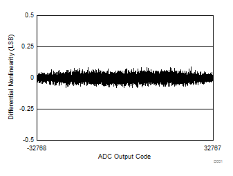
ADS8920B ADS8922B ADS8924B D001_SBAS729.gif
Typical DNL = ±0.2 LSB
Figure 6. Typical DNL
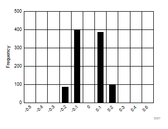
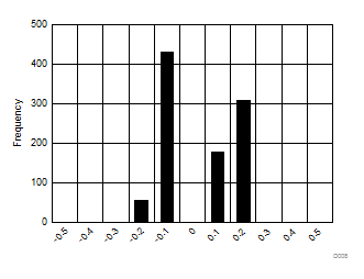
ADS8920B ADS8922B ADS8924B D007_SBAS729.gif
1000 devices
Figure 8. Typical DNL Distribution
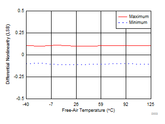
ADS8920B ADS8922B ADS8924B D003_SBAS729.gif
Figure 10. DNL vs Temperature
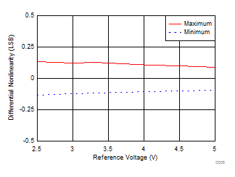
ADS8920B ADS8922B ADS8924B D005_SBAS729.gif
Figure 12. DNL vs Reference Voltage
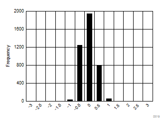
ADS8920B ADS8922B ADS8924B D019_SBAS729.gif
4000 devices
Figure 14. Typical Offset Distribution
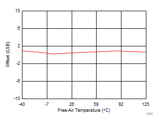
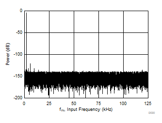
ADS8920B ADS8922B ADS8924B D020_SBAS729.gif
REF_SEL[2:0] = 000b
Figure 16. Offset vs Temperature
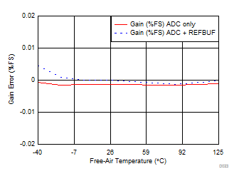
ADS8920B ADS8922B ADS8924B D023_SBAS729.gif
EN_MARG = 0b
Figure 18. Gain Error vs Temperature
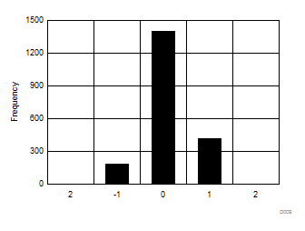
ADS8920B ADS8922B ADS8924B D009_SBAS729.gif
Standard Deviation = 0.47 LSB
Figure 20. DC Input Histogram
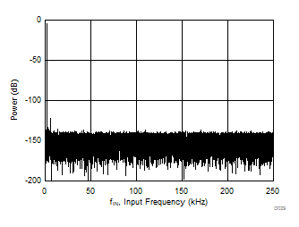
ADS8920B ADS8922B ADS8924B D029_SBAS729.gif
fIN = 2 kHz SNR = 96.8 dB THD = –125 dB
Figure 22. Typical FFT - ADS8922B
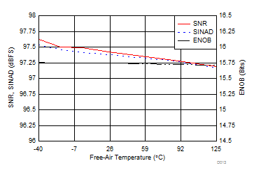
ADS8920B ADS8922B ADS8924B D013_SBAS729.gif
fIN = 2 kHz
Figure 24. Noise Performance vs Temperature
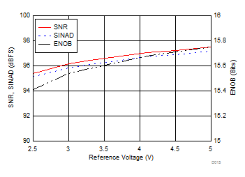
ADS8920B ADS8922B ADS8924B D015_SBAS729.gif
fIN = 2 kHz
Figure 26. Noise Performance vs Reference Voltage
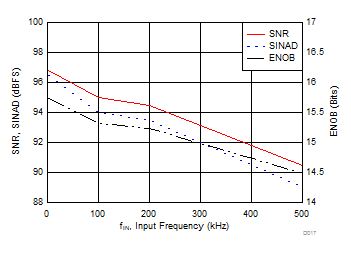
ADS8920B ADS8922B ADS8924B D017_SBAS729.gif
Figure 28. Noise Performance vs Input Frequency
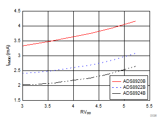
ADS8920B ADS8922B ADS8924B D026_SBAS729.gif
Figure 30. Analog Supply Current vs Supply Voltage
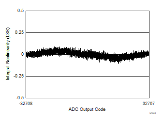
ADS8920B ADS8922B ADS8924B D002_SBAS729.gif
Typical INL = ±0.3 LSB
Figure 7. Typical INL
ADS8920B ADS8922B ADS8924B D008_SBAS729.gif
1000 devices
Figure 9. Typical INL Distribution
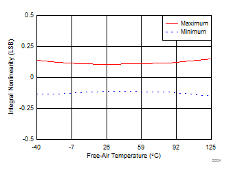
ADS8920B ADS8922B ADS8924B D004_SBAS729.gif
Figure 11. INL vs Temperature
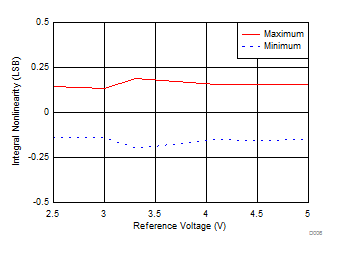
ADS8920B ADS8922B ADS8924B D006_SBAS729.gif
Figure 13. INL vs Reference Voltage
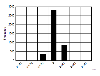
ADS8920B ADS8922B ADS8924B D022_SBAS729.gif
4000 devices
Figure 15. Typical Gain Error Distribution
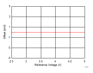
ADS8920B ADS8922B ADS8924B D021_SBAS729.gif
With appropriate REF_SEL[2:0], see OFST_CAL
Figure 17. Offset vs Reference Voltage
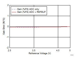
ADS8920B ADS8922B ADS8924B D024_SBAS729.gif
EN_MARG = 0b
Figure 19. Gain Error vs Reference Voltage
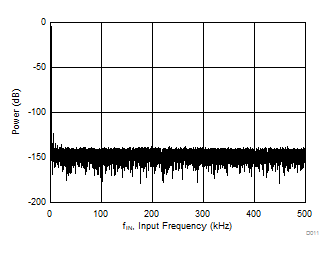
ADS8920B ADS8922B ADS8924B D011_SBAS729.gif
fIN = 2 kHz SNR = 96.8 dB THD = –125 dB
Figure 21. Typical FFT - ADS8920B
ADS8920B ADS8922B ADS8924B D030_SBAS729.gif
fIN = 2 kHz SNR = 96.8 dB THD = –125 dB
Figure 23. Typical FFT - ADS8924B
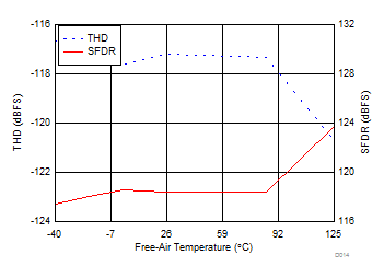
ADS8920B ADS8922B ADS8924B D014_SBAS729.gif
fIN = 2 kHz
Figure 25. Distortion Performance vs Temperature
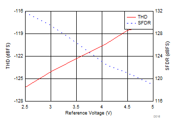
ADS8920B ADS8922B ADS8924B D016_SBAS729.gif
fIN = 2 kHz
Figure 27. Distortion Performance vs Reference Voltage
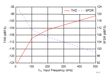
ADS8920B ADS8922B ADS8924B D018_SBAS729.gif
Figure 29. Distortion Performance vs Input Frequency
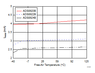
ADS8920B ADS8922B ADS8924B D028_SBAS729.gif
RVDD = 5 V
Figure 31. Analog Supply Current vs Temperature