ZHCSKR7A February 2020 – February 2020 ADS8355
PRODUCTION DATA.
- 1 特性
- 2 应用
- 3 说明
- 4 修订历史记录
- 5 Pin Configuration and Functions
- 6 Specifications
-
7 Detailed Description
- 7.1 Overview
- 7.2 Functional Block Diagram
- 7.3 Feature Description
- 7.4 Device Functional Modes
- 7.5 Programming
- 7.6
Register Map
- 7.6.1
ADS8355 Registers
- 7.6.1.1 PD_STANDBY Register (Offset = 4h) [reset = 0h]
- 7.6.1.2 PD_KEY Register (Offset = 5h) [reset = 0h]
- 7.6.1.3 SDO_CTRL Register (Offset = Dh) [reset = 0h]
- 7.6.1.4 DATA_OUT_CTRL Register (Offset = 11h) [reset = 0h]
- 7.6.1.5 REF_SEL Register (Offset = 20h) [reset = 0h]
- 7.6.1.6 REFDAC_A_LSB Register (Offset = 24h) [reset = 0h]
- 7.6.1.7 REFDAC_A_MSB Register (Offset = 25h) [reset = 0h]
- 7.6.1.8 REFDAC_B_LSB Register (Offset = 26h) [reset = 0h]
- 7.6.1.9 REFDAC_B_MSB Register (Offset = 27h) [reset = 0h]
- 7.6.1.10 INPUT_CONFIG Register (Offset = 28h) [reset = 0h]
- 7.6.1
ADS8355 Registers
- 8 Application and Implementation
- 9 Power Supply Recommendations
- 10Layout
- 11器件和文档支持
- 12机械、封装和可订购信息
7.5.1 Register Read/Write Operation
This device features configuration registers and supports the commands listed in Table 6 to access the internal configuration registers.
Table 6. Supported Commands
| B[19:16] | B[15:8] | B[7:0] | COMMAND ACRONYM | COMMAND DESCRIPTION |
|---|---|---|---|---|
| 0000 | 00000000000 | 00000000 | NOP | No operation. Next frame provides the ADC conversion result output on the SDO_X lines. |
| 0001 | <8-bit address> | <8-bit data> | WR_REG | Write <8-bit data> to the <8-bit address> |
| 0010 | <8-bit address> | 00000000 | RD_REG | Read contents from the <8-bit address> |
| 0011 | <8-bit address> | <8-bit unmasked bits> | SET_BITS | Set <8-bit unmasked bits> from <8-bit address> |
| 0100 | <8-bit address> | <8-bit unmasked bits> | CLR_BITS | Clear <8-bit unmasked bits> from <8-bit address> |
| Remaining combinations | xxxxxxxxx | xxxxxxxx | Reserved | These commands are reserved and treated by the device as no operation. |
The ADS8355 supports two types of data transfer operations: data write (the host controller configures the device), and data read (the host controller reads data from the device).
Any data write to the device is always synchronous to the external clock provided on the SCLK pin. The WR_REG command writes the 8-bit data into the 8-bit address specified in the command string. The CLR_BITS command clears the specified bits (identified by 1) at the 8-bit address (without affecting the other bits), and the SET_BITS command sets the specified bits (identified by 1) at the 8-bit address (without affecting the other bits).
Figure 31 shows the digital waveform for a register read operation. A register read operation consists of two frames: one frame to initiate a register read and a second frame to read data from the register address provided in the first frame. As shown in Figure 31, the 8-bit register address and the 8-bit dummy data are sent over the SDI pin during the first 20-bit frame with the read command (0010b). The 20-bit command information is right-aligned with the frame. If a command frame is smaller than 20 bits, the contents of the command are discarded. If a frame has more than 20 bits, the last 20 bits are used to decode the operation. When CS goes from low to high, this read command is decoded and the requested register data are available for reading during the next frame. During the second frame, the first eight bits on SDO_A correspond to the requested register read. During the second frame, SDI can be used to initiate another operation or can be set to 0.
 Figure 31. Register Read Operation
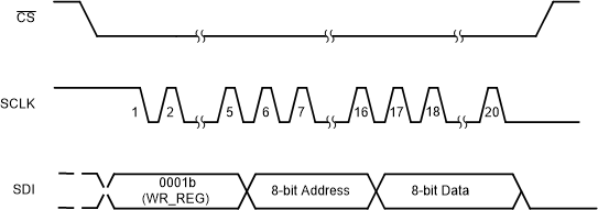
 Figure 32 shows that for writing data to the register, one 20-bit frame is required. The frame contents are right-aligned. If a command frame is smaller than 20 bits, the contents of the command are discarded. If a frame has more than 20 bits, the last 20 bits are used to decode the operation. The 20-bit data on SDI consists of a 4-bit write command (0001b), set bit command (0011b), or clear bit command (0100b), an 8-bit register address, and 8-bit data. The write command is decoded on the CS rising edge and the specified register is updated with the 8-bit data specified during the register write operation.
 Figure 32. Register Write Operation