SLAS611C October 2009 – January 2016 ADS5400
PRODUCTION DATA.
- 1 Features
- 2 Applications
- 3 Description
- 4 Revision History
- 5 Pin Configuration and Functions
- 6 Specifications
-
7 Detailed Description
- 7.1 Overview
- 7.2 Functional Block Diagram
- 7.3 Feature Description
- 7.4 Device Functional Modes
- 7.5 Programming
- 7.6 Register Maps
- 8 Application and Implementation
- 9 Power Supply Recommendations
- 10Layout
- 11Device and Documentation Support
- 12Mechanical, Packaging, and Orderable Information
封装选项
机械数据 (封装 | 引脚)
- PZP|100
散热焊盘机械数据 (封装 | 引脚)
- PZP|100
订购信息
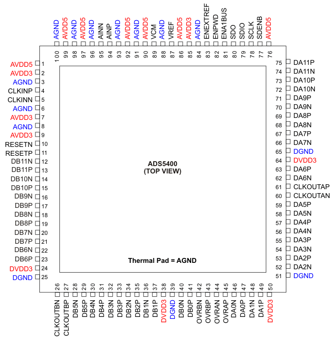
5 Pin Configuration and Functions
PZP Package
100-Pin HTQFP With Exposed Thermal Pad
Top View

Pin Functions
| PIN | TYPE | DESCRIPTION | |
|---|---|---|---|
| NO. | NAME | ||
| 3, 6, 8, 84, 88, 91, 93, 96, 98, 100 | AGND | Ground | Analog ground |
| 94, 95 | AINP, AINN | Input | Analog differential input signal (positive, negative). Includes 100-Ω differential load on-chip. |
| 2, 7, 9, 85 | AVDD3 | Supply | Analog power supply (3.3 V) |
| 1, 76, 86, 90, 92, 97, 99 | AVDD5 | Supply | Analog power supply (5 V) |
| 4, 5 | CLKINP, CLKINN | Input | Differential input clock (positive, negative). Includes 160-Ω differential load on-chip. |
| 60, 61 | CLKOUTAN, CLKOUTAP | Output | Bus A, Clock output (Data ready), LVDS output pair |
| 26, 27 | CLKOUTBN, CLKOUTBP | Output | Bus B, Clock output (Data ready), LVDS output pair |
| 46, 47 | DA0N, DA0P | Output | Bus A, LVDS digital output pair, least-significant bit (LSB) (P = positive output, N = negative output) |
| 48-49, 52-59, 62-63, 66-73 | DA1N–DA10N, DA1P-DA10P | Output | Bus A, LVDS digital output pairs (bits 1- 10) |
| 74, 75 | DA11N, DA11P | Output | Bus A, LVDS digital output pair, most-significant bit (MSB) |
| 40, 41 | DB0N, DB0P | Output | Bus B, LVDS digital output pair, least-significant bit (LSB) (P = positive output, N = negative output) |
| 14-23, 28-37 | DB1N–DB10N, DB1P-DB10P | Output | Bus B, LVDS digital output pairs (bits 1- 10) |
| 12, 13 | DB11N, DB11P | Output | Bus B, LVDS digital output pair, most-significant bit (MSB) |
| 25, 39, 51, 65 | DGND | Ground | Digital ground |
| 24, 38, 50, 64 | DVDD3 | Supply | Output driver power supply (3.3 V) |
| 81(1) | ENA1BUS | Input | Enable single output bus mode (2-bus mode is default), active high. This pin is logic OR'd with addr 0x02h bit<0>. |
| 83(1) | ENEXTREF | Input | Enable External Reference Mode, active high. Device uses an external voltage reference when high. This pin is logic OR'd with addr 0x05h bit<2>. |
| 82(1) | ENPWD | Input | Enable Powerdown, active high. Places the converter into power-saving sleep mode when high. This pin is logic OR'd with addr 0x05h bit<6>. |
| 44, 45 | OVRAN, OVRAP | Output | Bus A, Overrange indicator LVDS output. A logic high signals an analog input in excess of the full-scale range. Becomes SYNCOUTA when SYNC mode is enabled in register 0x05. |
| 42, 43 | OVRBN, OVRBP | Output | Bus B, Overrange indicator LVDS output. A logic high signals an analog input in excess of the full-scale range. Becomes SYNCOUTB when SYNC mode is enabled in register 0x05. |
| 10, 11 | RESETN, RESETP | Input | Digital Reset Input, LVDS input pair. Inactive if logic low. When clocked in a high state, this is used for resetting the polarity of CLKOUT signal pair(s). If SYNC mode is enabled in register 0x05, this input also provides a SYNC time-stamp with the data sample present when RESET is clocked by the ADC, as well as CLKOUT polarity reset. Includes 100-Ω differential load on-chip. |
| 78 | SCLK | Input | Serial interface clock. |
| 77 | SDENB | Input | Active low serial data enable, always an input. Use to enable the serial interface. Internal 100kΩ pull-up resistor. |
| 79 | SDIO | Input/Output | Bidirectional serial interface data in 3-pin mode (default) for programming/reading internal registers. In 4-pin interface mode (reg 0x01), the SDIO pin is an input only. |
| 80 | SDO | Output | Unidirectional serial interface data in 4-pin mode (reg 0x01) provides internal register settings. The SDO pin is in high-impedance state in 3-pin interface mode (default). |
| 89 | VCM | Input/Output | Analog input common mode voltage, Output (for DC-coupled applications, nominally 2.5 V). A 0.1-μF capacitor to AGND is recommended, but not required. |
| 87 | VREF | Input | Reference voltage input (2 V nominal). A 0.1-μF capacitor to AGND is recommended, but not required. |