SLAS669E September 2010 – may 2020 ADS5400-SP
PRODUCTION DATA.
- 1 Features
- 2 Applications
- 3 Description
- 4 Revision History
- 5 Pin Configuration and Functions
- 6 Specifications
-
7 Detailed Description
- 7.1 Overview
- 7.2 Functional Block Diagram
- 7.3 Feature Description
- 7.4 Device Functional Modes
- 7.5 Programming
- 7.6 Serial Register Map
- 8 Application and Implementation
- 9 Power Supply Recommendations
- 10Layout
- 11Device and Documentation Support
- 12Mechanical, Packaging, and Orderable Information
7.5.1 Serial Interface
The serial port of the ADS5400-SP is a flexible serial interface which communicates with industry standard microprocessors and microcontrollers. The interface provides read/write access to all registers used to define the operating modes of ADS5400. It is compatible with most synchronous transfer formats and can be configured as a 3 or 4 pin interface in register 0x01h. In both configurations, SCLK is the serial interface input clock and SDENB is serial interface enable. For 3 pin configuration, SDIO is a bidirectional pin for both data in and data out. For 4 pin configuration, SDIO is data in only and SDO is data out only.
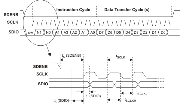
Each read/write operation is framed by signal SDENB (Serial Data Enable Bar) asserted low for 2 to 5 bytes, depending on the data length to be transferred (1–4 bytes). The first frame byte is the instruction cycle which identifies the following data transfer cycle as read or write, how many bytes to transfer, and what address to transfer the data. Table 2 indicates the function of each bit in the instruction cycle and is followed by a detailed description of each bit. Frame bytes 2 to 5 comprise the data transfer cycle.
Table 2. Instruction Byte of the Serial Interface
| MSB | LSB |
| Bit | 7 | 6 | 5 | 4 | 3 | 2 | 1 | 0 |
| Description | R/W | N1 | N0 | A4 | A3 | A2 | A1 | A0 |
| R/W | Identifies the following data transfer cycle as a read or write operation. A high indicates a read operation from ADS5400 and a low indicates a write operation to the ADS5400. | |||||||
| [N1:N0] | Identifies the number of data bytes to be transferred per Table 3 below. Data is transferred MSB first. | |||||||
Table 3. Number of Transferred Bytes Within One Communication Frame
| N1 | N0 | Description |
|---|---|---|
| 0 | 0 | Transfer 1 Byte |
| 0 | 1 | Transfer 2 Bytes |
| 1 | 0 | Transfer 3 Bytes |
| 1 | 1 | Transfer 4 Bytes |
| [A4:A0] | Identifies the address of the register to be accessed during the read or write operation. For multi-byte transfers, this address is the starting address. Note that the address is written to the ADS5400 MSB first and counts down for each byte. | |||||||
Figure 36 shows the serial interface timing diagram for a device write operation. SCLK is the serial interface clock input to ADS5400-SP. Serial data enable SDENB is an active low input to ADS5400-SP. SDIO is serial data in. Input data to the device is clocked on the rising edges of SCLK.
 Figure 36. Serial Interface Write Timing Diagram
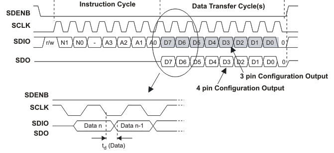
 Figure 37 shows the serial interface timing diagram for a device read operation. SCLK is the serial interface clock input to the device. Serial data enable SDENB is an active low input to the device. SDIO is serial data in during the instruction cycle. In 3 pin configuration, SDIO is data out from the device during the data transfer cycle(s), while SDO is in a high-impedance state. In 4 pin configuration, SDO is data out from the device during the data transfer cycle(s). At the end of the data transfer, SDO outputs low on the final falling edge of SCLK until the rising edge of SDENB when it will 3-state.
 Figure 37. Serial Interface Read Timing Diagram