ZHCSI83C may   2018  – may 2023 ADC12DL3200

PRODUCTION DATA  

  1.   1
  2. 1特性
  3. 2应用
  4. 3说明
  5. 4Revision History
  6. 5Pin Configuration and Functions
  7. 6Specifications
    1. 6.1  Absolute Maximum Ratings
    2. 6.2  ESD Ratings
    3. 6.3  Recommended Operating Conditions
    4. 6.4  Thermal Information
    5. 6.5  Electrical Characteristics: DC Specifications
    6. 6.6  Electrical Characteristics: Power Consumption
    7. 6.7  Electrical Characteristics: AC Specifications (Dual-Channel Mode)
    8. 6.8  Electrical Characteristics: AC Specifications (Single-Channel Mode)
    9. 6.9  Timing Requirements
    10. 6.10 Switching Characteristics
    11. 6.11 Typical Characteristics
  8. 7Detailed Description
    1. 7.1 Overview
    2. 7.2 Functional Block Diagram
    3. 7.3 Feature Description
      1. 7.3.1 Analog Inputs
        1. 7.3.1.1 Analog Input Protection
        2. 7.3.1.2 Full-Scale Voltage (VFS) Adjustment
        3. 7.3.1.3 Analog Input Offset Adjust
      2. 7.3.2 ADC Core
        1. 7.3.2.1 ADC Theory of Operation
        2. 7.3.2.2 ADC Core Calibration
        3. 7.3.2.3 ADC Overrange Detection
        4. 7.3.2.4 Code Error Rate (CER)
        5. 7.3.2.5 Internal Dither
      3. 7.3.3 Timestamp
      4. 7.3.4 Clocking
        1. 7.3.4.1 Noiseless Aperture Delay Adjustment (tAD Adjust)
        2. 7.3.4.2 Aperture Delay Ramp Control (TAD_RAMP)
        3. 7.3.4.3 SYSREF Capture for Multi-Device Synchronization and Deterministic Latency
          1. 7.3.4.3.1 SYSREF Position Detector and Sampling Position Selection (SYSREF Windowing)
          2. 7.3.4.3.2 Automatic SYSREF Calibration
      5. 7.3.5 LVDS Digital Interface
        1. 7.3.5.1 Multi-Device Synchronization and Deterministic Latency Using Strobes
          1. 7.3.5.1.1 Dedicated Strobe Pins
          2. 7.3.5.1.2 Reduced Width Interface With Dedicated Strobe Pins
          3. 7.3.5.1.3 LSB Replacement With a Strobe
          4. 7.3.5.1.4 Strobe Over All Data Pairs
      6. 7.3.6 Alarm Monitoring
        1. 7.3.6.1 Clock Upset Detection
      7. 7.3.7 Temperature Monitoring Diode
      8. 7.3.8 Analog Reference Voltage
    4. 7.4 Device Functional Modes
      1. 7.4.1 Dual-Channel Mode (Non-DES Mode)
      2. 7.4.2 Internal Dither Modes
      3. 7.4.3 Single-Channel Mode (DES Mode)
      4. 7.4.4 LVDS Output Driver Modes
      5. 7.4.5 LVDS Output Modes
        1. 7.4.5.1 Staggered Output Mode
        2. 7.4.5.2 Aligned Output Mode
        3. 7.4.5.3 Reducing the Number of Strobes
        4. 7.4.5.4 Reducing the Number of Data Clocks
        5. 7.4.5.5 Scrambling
        6. 7.4.5.6 Digital Interface Test Patterns and LVSD SYNC Functionality
          1. 7.4.5.6.1 Active Pattern
          2. 7.4.5.6.2 Synchronization Pattern
          3. 7.4.5.6.3 User-Defined Test Pattern
      6. 7.4.6 Power-Down Modes
      7. 7.4.7 Calibration Modes and Trimming
        1. 7.4.7.1 Foreground Calibration Mode
        2. 7.4.7.2 Background Calibration Mode
        3. 7.4.7.3 Low-Power Background Calibration (LPBG) Mode
      8. 7.4.8 Offset Calibration
      9. 7.4.9 Trimming
    5. 7.5 Programming
      1. 7.5.1 Using the Serial Interface
        1. 7.5.1.1 SCS
        2. 7.5.1.2 SCLK
        3. 7.5.1.3 SDI
        4. 7.5.1.4 SDO
        5. 7.5.1.5 78
        6. 7.5.1.6 Streaming Mode
        7. 7.5.1.7 80
    6. 7.6 Register Maps
      1. 7.6.1 SPI_REGISTER_MAP Registers
  9.   Application and Implementation
    1. 8.1 Application Information
    2. 8.2 Typical Applications
      1. 8.2.1 Wideband RF Sampling Receiver
        1. 8.2.1.1 Design Requirements
          1. 8.2.1.1.1 Input Signal Path
          2. 8.2.1.1.2 Clocking
        2. 8.2.1.2 Detailed Design Procedure
          1. 8.2.1.2.1 Calculating Values of AC-Coupling Capacitors
        3. 8.2.1.3 Application Curves
      2. 8.2.2 Reconfigurable Dual-Channel, 2.5-GSPS or Single-Channel, 5.0-GSPS Oscilloscope
        1. 8.2.2.1 Design Requirements
          1. 8.2.2.1.1 Input Signal Path
          2. 8.2.2.1.2 Clocking
          3. 8.2.2.1.3 The ADC12DL3200
        2. 8.2.2.2 Application Curves
    3. 8.3 Initialization Set Up
    4. 8.4 Power Supply Recommendations
      1. 8.4.1 Power Sequencing
    5. 8.5 Layout
      1. 8.5.1 Layout Guidelines
      2. 8.5.2 Layout Example
  10. 8Device and Documentation Support
    1. 8.1 Device Support
      1. 8.1.1 Development Support
    2. 8.2 接收文档更新通知
    3. 8.3 支持资源
    4. 8.4 商标
    5. 8.5 静电放电警告
    6. 8.6 术语表
  11. 9Mechanical, Packaging, and Orderable Information

封装选项

机械数据 (封装 | 引脚)
散热焊盘机械数据 (封装 | 引脚)
订购信息
Calculating Values of AC-Coupling Capacitors

AC-coupling capacitors are used in the input CLK± pair. The capacitor values must be large enough to address the lowest frequency signals of interest, but not so large as to cause excessively long startup biasing times, or unwanted parasitic inductance.

The minimum capacitor value can be calculated based on the lowest frequency signal that is transferred through the capacitor. Given a 50-Ω, single-ended clock or data path impedance, good practice is to set the capacitor impedance to be less than 1 Ω at the lowest frequency of interest. This setting ensures minimal impact on signal level at that frequency. For the CLK± path, the minimum-rated clock frequency is 800 MHz. Therefore, the minimum capacitor value can be calculated from:

Equation 3. GUID-C8525C6A-327B-4FBB-B072-61C55A50206C-low.gif

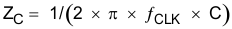
Setting Zc = 1 Ω and rearranging gives:

Equation 4. GUID-F48447AE-10D2-4359-87E9-81FDD56082A4-low.gif

Therefore, a capacitance value of at least 199 pF is needed to provide the low-frequency response for the CLK± path. If the minimum clock frequency is higher than 800 MHz, this calculation can be revisited for that frequency. Capacitors must also be selected for good response at high frequencies, usually identified by low inductance or high self-resonance frequency, and with dimensions that match the high-frequency signal traces they are connected to. Capacitors of the 0201 size are frequently well-suited to these applications.