ZHCSI83C may 2018 – may 2023 ADC12DL3200
PRODUCTION DATA
- 1
- 1特性
- 2应用
- 3说明
- 4Revision History
- 5Pin Configuration and Functions
-
6Specifications
- 6.1 Absolute Maximum Ratings
- 6.2 ESD Ratings
- 6.3 Recommended Operating Conditions
- 6.4 Thermal Information
- 6.5 Electrical Characteristics: DC Specifications
- 6.6 Electrical Characteristics: Power Consumption
- 6.7 Electrical Characteristics: AC Specifications (Dual-Channel Mode)
- 6.8 Electrical Characteristics: AC Specifications (Single-Channel Mode)
- 6.9 Timing Requirements
- 6.10 Switching Characteristics
- 6.11 Typical Characteristics
-
7Detailed Description
- 7.1 Overview
- 7.2 Functional Block Diagram
- 7.3
Feature Description
- 7.3.1 Analog Inputs
- 7.3.2 ADC Core
- 7.3.3 Timestamp
- 7.3.4 Clocking
- 7.3.5 LVDS Digital Interface
- 7.3.6 Alarm Monitoring
- 7.3.7 Temperature Monitoring Diode
- 7.3.8 Analog Reference Voltage
- 7.4
Device Functional Modes
- 7.4.1 Dual-Channel Mode (Non-DES Mode)
- 7.4.2 Internal Dither Modes
- 7.4.3 Single-Channel Mode (DES Mode)
- 7.4.4 LVDS Output Driver Modes
- 7.4.5 LVDS Output Modes
- 7.4.6 Power-Down Modes
- 7.4.7 Calibration Modes and Trimming
- 7.4.8 Offset Calibration
- 7.4.9 Trimming
- 7.5 Programming
- 7.6 Register Maps
- Application and Implementation
- 8Device and Documentation Support
- 9Mechanical, Packaging, and Orderable Information
封装选项
机械数据 (封装 | 引脚)
散热焊盘机械数据 (封装 | 引脚)
订购信息
6.10 Switching Characteristics
typical values at TA = +25°C, nominal supply voltages, default full-scale voltage (FS_RANGE_A = FS_RANGE_B = 0xA000), fIN = 248 MHz, AIN = –1 dBFS, fCLK = maximum rated clock frequency, filtered 1-VPP-DIFF sine-wave clock, DES_EN = 1, LDEMUX = 1, LALIGNED = 0, ADC_DITH = 0x01, LVDS driver high-swing mode (HSM), background calibration (unless otherwise noted); minimum and maximum values are at nominal supply voltages and over operating free-air temperature range provided in the Recommended Operating Conditions table
| PARAMETER | TEST CONDITIONS | MIN | TYP | MAX | UNIT | |
|---|---|---|---|---|---|---|
| DEVICE (SAMPLING) CLOCK (CLK+, CLK–) | ||||||
| tAD | Sampling (aperture) delay from CLK± rising edge (dual channel mode) or rising and falling edge (single channel mode) to sampling instant(4) | TAD_COARSE = 0x00, TAD_FINE = 0x00 and TAD_INV = 0 | 360 | ps | ||
| tAD(MAX) | Maximum tAD Adjust programmable delay, not including clock inversion (TAD_INV = 0) | Coarse adjustment (TAD_COARSE = 0xFF) | 289 | ps | ||
| Fine adjustment (TAD_FINE = 0xFF) | 4.9 | |||||
| tAD(STEP) | Aperture delay step size | Coarse adjustment (TAD_COARSE) | 1.13 | ps | ||
| Fine adjustment (TAD_FINE) | 19 | fs | ||||
| tAJ | Aperture jitter, rms | Minimum tAD Adjust coarse setting (TAD_COARSE = 0x00, TAD_INV = 0), dither disabled (ADC_DITH_EN = 0) | 55 | fs | ||
| Minimum tAD Adjust coarse setting (TAD_COARSE = 0xFF, TAD_INV = 0), dither enabled (ADC_DITH_EN = 1) | 70 | |||||
| Maximum tAD Adjust coarse setting (TAD_COARSE = 0xFF) excluding TAD_INV (TAD_INV = 0), dither disabled (ADC_DITH_EN = 0) | 70(1) | |||||
| Maximum tAD Adjust coarse setting (TAD_COARSE = 0xFF) excluding TAD_INV (TAD_INV = 0), dither enabled (ADC_DITH_EN = 1) | 80(1) | |||||
| LVDS OUTPUTS (DACLK±, DASTR±, DA[11:0]±, DBCLK±, DBSTR±, DB[11:0]±, DCCLK±, DCSTR±, DC[11:0]±, DDCLK±, DDSTR±, DD[11:0]±) | ||||||
| fBIT | Output bit rate per output data pair | 1.6 | Gbps | |||
| fDCLK | DDR data clock frequency | 800 | MHz | |||
| tDJ | DDR data clock total jitter, peak-to-peak, with random jitter portion defined with respect to a BER=1e–15 (Q=7.94) | UPAT_CTRL = 0x10 | 36 | ps | ||
| tSKEW(SAME) | Maximum timing skew between any two LVDS output pairs (DxCLK±, Dx[11:0]±, DxSTR±) within the same LVDS bank over operating conditions | 75 | ps | |||
| tSKEW(ALL) | Maximum timing skew between any two LVDS output pairs (DxCLK±, Dx[11:0]±, DxSTR±) in all LVDS banks over operating conditions with tOSAB, tOSAC and tOSBD skew excluded | 125 | ps | |||
| tOSAB | Functional timing offset between DACLK± rising edge and DBCLK± rising edge, positive number indicates that DACLK± leads DBCLK± | DES_EN = 0, LDEMUX = 0, LALIGNED = 0 | 0 | tCLK | ||
| DES_EN = 0, LDEMUX = 0, LALIGNED = 1 | 0 | |||||
| DES_EN = 0, LDEMUX = 1, LALIGNED = 0 | 0 | |||||
| DES_EN = 0, LDEMUX = 1, LALIGNED = 1 | 0 | |||||
| DES_EN = 1, LDEMUX = 0, LALIGNED = 0 | 0.5 | |||||
| DES_EN = 1, LDEMUX = 0, LALIGNED = 1 | 0 | |||||
| DES_EN = 1, LDEMUX = 1, LALIGNED = 0 | 0.5 | |||||
| DES_EN = 1, LDEMUX = 1, LALIGNED = 1 | 0 | |||||
| tOSAC | Functional timing offset between DACLK± rising edge and DCCLK± rising edge, positive number indicates that DACLK± leads DCCLK± | DES_EN = 0, LDEMUX = 1, LALIGNED = 0 | 1 | tCLK | ||
| DES_EN = 0, LDEMUX = 1, LALIGNED = 1 | 0 | |||||
| DES_EN = 1, LDEMUX = 1, LALIGNED = 0 | 1 | |||||
| DES_EN = 1, LDEMUX = 1, LALIGNED = 1 | 0 | |||||
| tOSBD | Functional timing offset between DBCLK± rising edge and DDCLK± rising edge, positive number indicates that DBCLK± leads DDCLK± | DES_EN = 0, LDEMUX = 1, LALIGNED = 0 | 1 | tCLK | ||
| DES_EN = 0, LDEMUX = 1, LALIGNED = 1 | 0 | |||||
| DES_EN = 1, LDEMUX = 1, LALIGNED = 0 | 1 | |||||
| DES_EN = 1, LDEMUX = 1, LALIGNED = 1 | 0 | |||||
| tTLH | Low-to-high transition time (differential) | 20% to 80%, 1.6 Gbps, VLVDS = 1.9 V, UPAT_CTRL = 0x10 | 125 | ps | ||
| 20% to 80%, 1.6 Gbps, VLVDS = 1.1 V, UPAT_CTRL = 0x10 | 200 | |||||
| tTHL | High-to-low transition time (differential) | 80% to 20%, 1.6 Gbps, VLVDS = 1.9 V, UPAT_CTRL = 0x10 | 125 | ps | ||
| 80% to 20%, 1.6 Gbps, VLVDS = 1.1 V, UPAT_CTRL = 0x10 | 200 | |||||
| LATENCY | ||||||
| tOD | Output delay from CLK± rising edge (dual-channel mode) or falling edge (single-channel mode) to DACLK± output(4) | TAD_COARSE = 0x00, TAD_FINE = 0x00 and TAD_INV = 0 | 1.5 | ns | ||
| tLAT(DIG) | CLK± edge that samples input signal to CLK± edge that launches data, digital latency only(2)(4) | DES_EN = 0, LDEMUX = 0, LALIGNED = 0 | 26 | tCLK | ||
| DES_EN = 0, LDEMUX = 0, LALIGNED = 1 | 26 | |||||
| DES_EN = 0, LDEMUX = 1, LALIGNED = 0 | 26 | |||||
| DES_EN = 0, LDEMUX = 1, LALIGNED = 1 | 27 | |||||
| DES_EN = 1, LDEMUX = 0, LALIGNED = 0 | 26 | |||||
| DES_EN = 1, LDEMUX = 0, LALIGNED = 1 | 26.5 | |||||
| DES_EN = 1, LDEMUX = 1, LALIGNED = 0 | 26 | |||||
| DES_EN = 1, LDEMUX = 1, LALIGNED = 1 | 27.5 | |||||
| tLAT(STB) | Latency from SYSREF± being sampled by rising edge of CLK± to the start of the corresponding data frame(3) | DES_EN = 0, LDEMUX = 0, LALIGNED = 0 | 47 | tCLK | ||
| DES_EN = 0, LDEMUX = 0, LALIGNED = 1 | 47 | |||||
| DES_EN = 0, LDEMUX = 1, LALIGNED = 0 | 47 | |||||
| DES_EN = 0, LDEMUX = 1, LALIGNED = 1 | 48 | |||||
| DES_EN = 1, LDEMUX = 0, LALIGNED = 0 | 46.5 | |||||
| DES_EN = 1, LDEMUX = 0, LALIGNED = 1 | 47 | |||||
| DES_EN = 1, LDEMUX = 1, LALIGNED = 0 | 46.5 | |||||
| DES_EN = 1, LDEMUX = 1, LALIGNED = 1 | 48 | |||||
| tLAT( SYNCSE) | Latency from SYNCSE assertion or deassertion to DB0± (LSB) changing from normal data to strobe output or strobe output to normal data, digital latency only | LDEMUX = 0 | 26 | 36+1*LFRAME | tCLK | |
| LDEMUX = 1 | 26 | 36+2*LFRAME | ||||
| SERIAL PROGRAMMING INTERFACE (SDO) | ||||||
| t(OZD) | Delay from falling edge of 16th SCLK cycle during read operation for SDO transition from tri-state to valid data | 1 | ns | |||
| t(ODZ) | Delay from SCS rising edge for SDO to transition from valid data to tri-state | 10 | ns | |||
| t(OD) | Delay from falling edge of SCLK during read operation to SDO valid | 1 | 10 | ns | ||
(1) tAJ increases because of additional attenuation on internal clock path.
(2) When LDEMUX = 1 the output buses are aligned in time requiring the earlier sample(s) to be delayed before outputting on the LVDS buses to align with the later samples. The latency for the buses will be slightly different due to added delays. The number shown is for the worst case bus.
(3) When LDEMUX = 0 the output buses are staggered in time and therefore the start of data frames occur at staggered times. The number shown is for the earliest output frame. The strobe signals are output at the end of a frame so the start of a data frame corresponds to the data output immediately after a strobe output.
(4) Both tAD and tOD increase by the delay introduced by TAD_COARSE, TAD_FINE and TAD_INV when tAD Adjust is used to delay the sampling instant. The total latency through the device does not include the aperture delay. Total latency through device is tLAT = tLAT(DIG) + tOD - tAD.
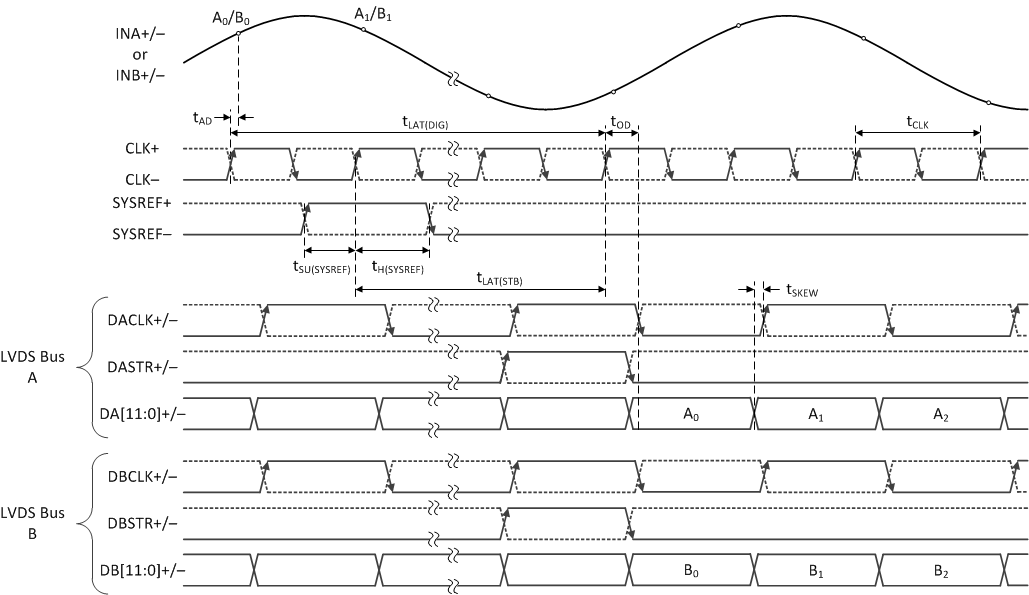
tSU(SYSREF) and tH(SYSREF) are only shown for completeness. Use automatic SYSREF calibration or SYSREF windowing to meet SYSREF timing.
Figure 6-1 Dual-Channel, 2-Bus Mode Timing (LDEMUX = 0, DES_EN = 0, LALIGNED = 0 or 1)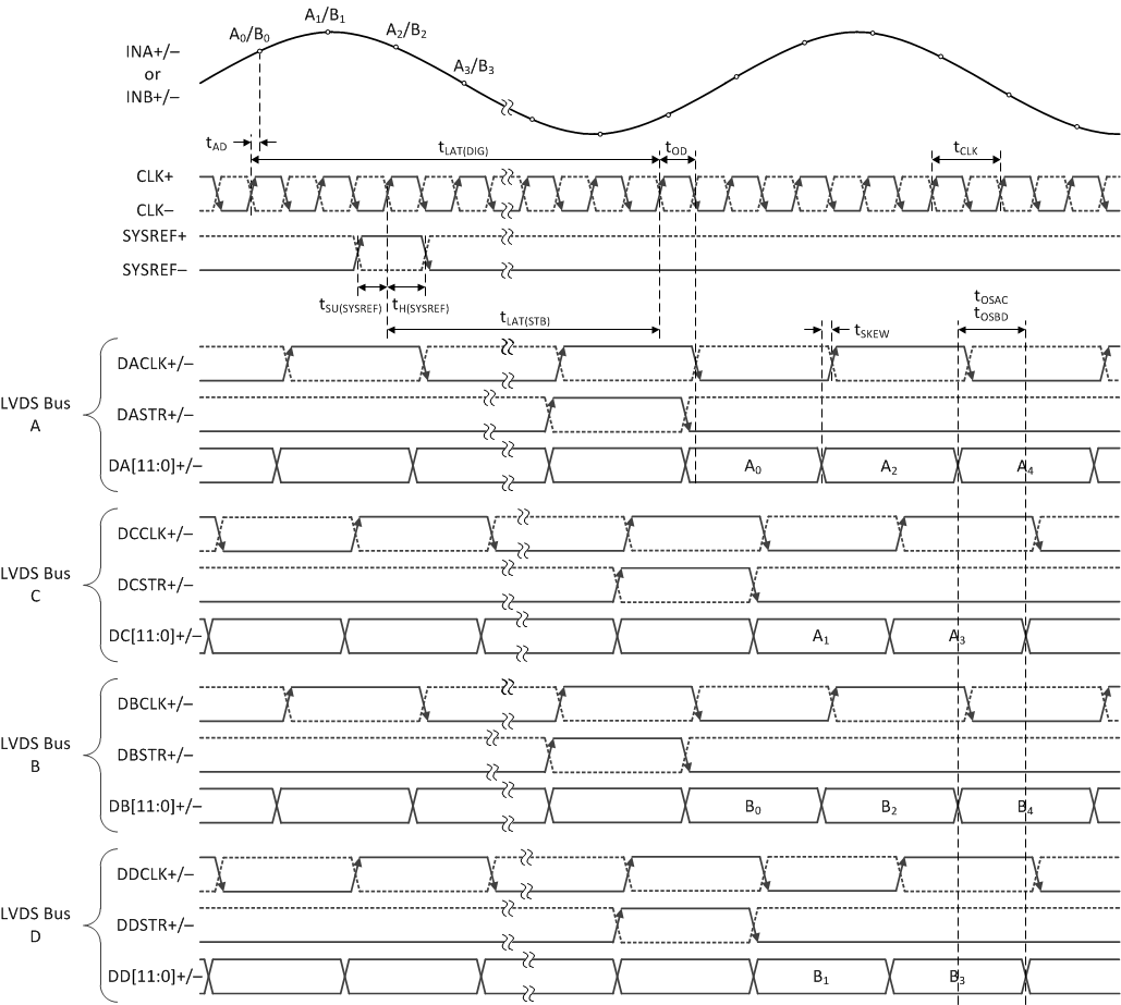
tSU(SYSREF) and tH(SYSREF) are only shown for completeness. Use automatic SYSREF calibration or SYSREF windowing to meet SYSREF timing.
Figure 6-2 Dual-Channel, 4-Bus, Staggered-Mode Timing (LDEMUX = 1, DES_EN = 0, LALIGNED = 0)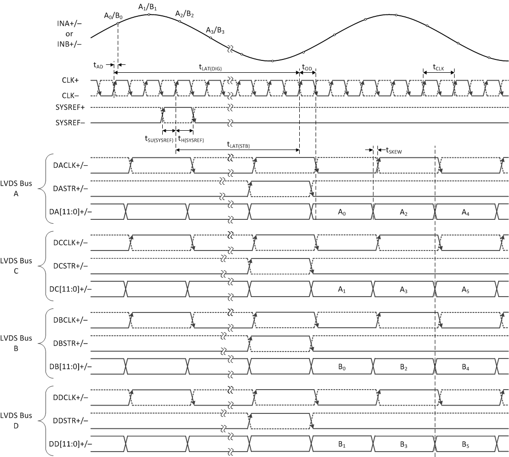
tSU(SYSREF) and tH(SYSREF) are only shown for completeness. Use automatic SYSREF calibration or SYSREF windowing to meet SYSREF timing.
Figure 6-3 Dual-Channel, 4-Bus, Aligned-Mode Timing (LDEMUX = 1, DES_EN = 0, LALIGNED = 1)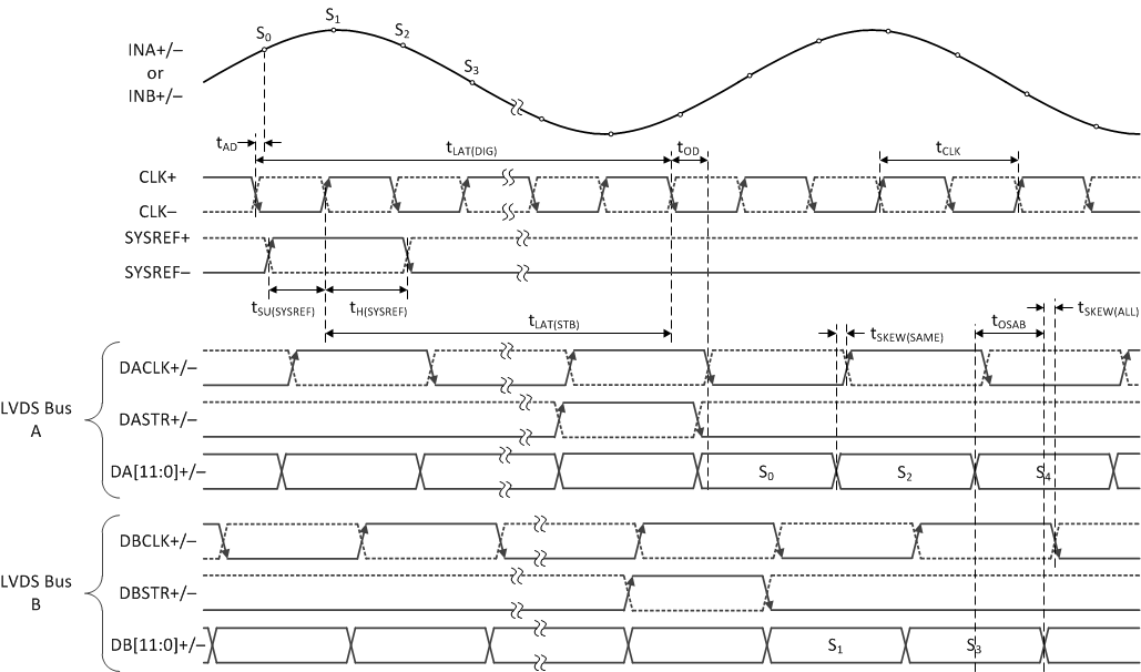
tSU(SYSREF) and tH(SYSREF) are only shown for completeness. Use automatic SYSREF calibration or SYSREF windowing to meet SYSREF timing.
Figure 6-4 Single-Channel, 2-Bus, Staggered-Mode Timing (LDEMUX = 0, DES_EN = 1, LALIGNED = 0)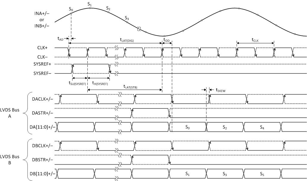
tSU(SYSREF) and tH(SYSREF) are only shown for completeness. Use automatic SYSREF calibration or SYSREF windowing to meet SYSREF timing.
Figure 6-5 Single-Channel, 2-Bus, Aligned-Mode Timing (LDEMUX = 0, DES_EN = 1, LALIGNED = 1)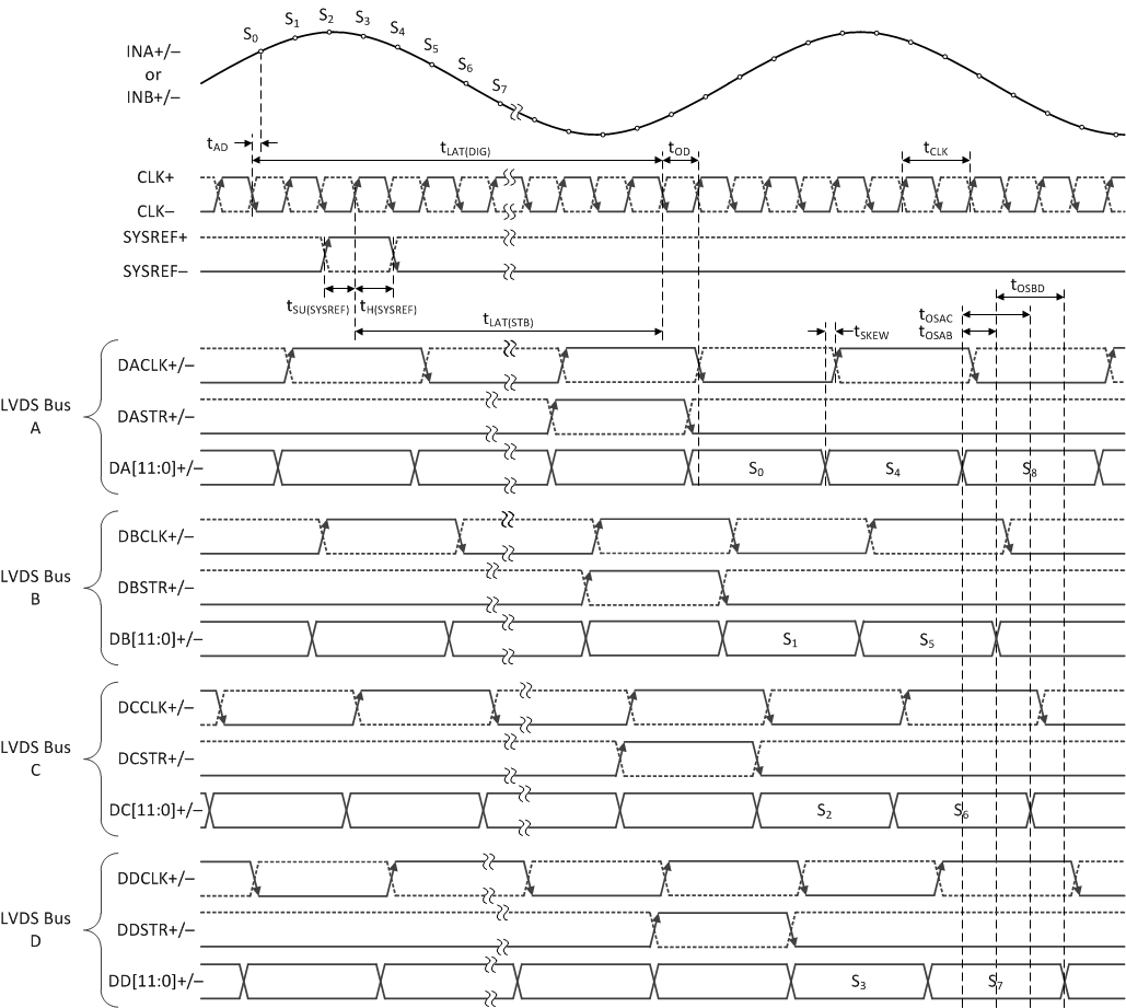
tSU(SYSREF) and tH(SYSREF) are only shown for completeness. Use automatic SYSREF calibration or SYSREF windowing to meet SYSREF timing.
Figure 6-6 Single-Channel, 4-Bus, Staggered-Mode Timing (LDEMUX = 1, DES_EN = 1, LALIGNED = 0)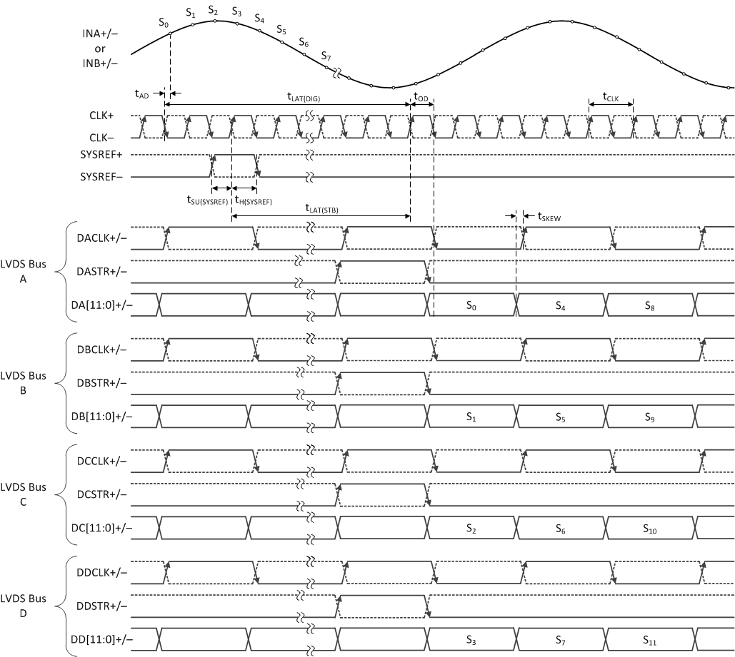
tSU(SYSREF) and tH(SYSREF) are only shown for completeness. Use automatic SYSREF calibration or SYSREF windowing to meet SYSREF timing.
Figure 6-7 Single-Channel, 4-Bus, Aligned-Mode Timing (LDEMUX = 1, DES_EN = 1, LALIGNED = 1)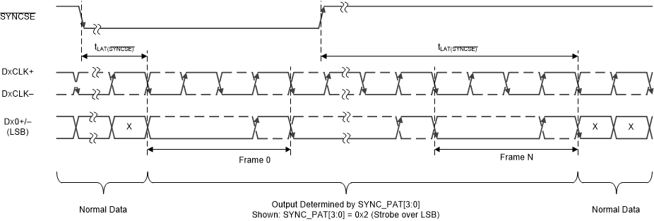 Figure 6-8 SYNCSE Timing Diagram
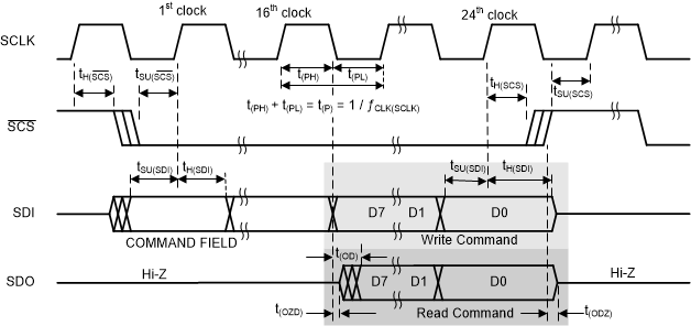 Figure 6-9 Serial Interface Timing