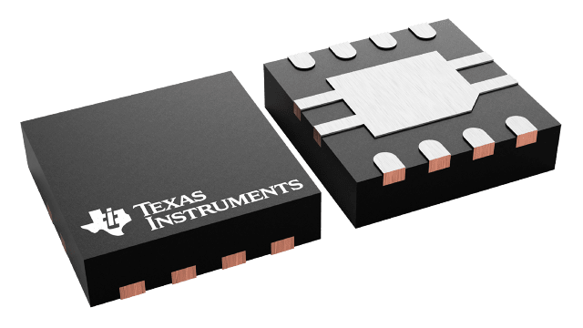
封装信息
| 封装 | 引脚 VSON (DRB) | 8 |
| 工作温度范围 (°C) -40 to 85 |
| 包装数量 | 包装 3,000 | LARGE T&R |
TPA2006D1 的特性
- Maximum Battery Life and Minimum Heat
- Efficiency With an 8-Ω Speaker:
- 88% at 400 mW
- 80% at 100 mW
- 2.8-mA Quiescent Current
- 0.5-µA Shutdown Current
- Efficiency With an 8-Ω Speaker:
- SHUTDOWN Pin has 1.8-V Compatible
Thresholds - Capable of Driving an
8-Ω Speaker (2.5 V ≤ VDD ≤ 5.5 V) and a
4-Ω Speaker (2.5 V ≤ VDD ≤ 4.2 V) - Only Three External Components
- Optimized PWM Output Stage Eliminates LC
Output Filter - Internally Generated 250-kHz Switching
Frequency Eliminates Capacitor and Resistor - Improved PSRR (–75 dB) and Wide Supply
Voltage (2.5 V to 5.5 V) Eliminates Need for a
Voltage Regulator - Fully Differential Design Reduces RF
Rectification and Eliminates Bypass Capacitor - Improved CMRR Eliminates Two Input
Coupling Capacitors
- Optimized PWM Output Stage Eliminates LC
- Space-Saving 3 mm x 3 mm VSON Package
(DRB)
TPA2006D1 的说明
The TPA2006D1 device is a 1.45-W high efficiency filter-free class-D audio power amplifier in a 3 mm × 3 mm VSON package that requires only three external components. The SHUTDOWN pin is fully compatible with 1.8-V logic GPIO, such as are used on low-power cellular chipsets.
Features like 88% efficiency, –75-dB PSRR, improved RF-rectification immunity, and small total PCB footprint make the TPA2006D1 device ideal for cellular handsets. A fast start-up time of 1 ms with minimal pop makes the TPA2006D1 device ideal for PDA applications.
In cellular handsets, the earpiece, speaker phone, and melody ringer can each be driven by the TPA2006D1 device. The TPA2006D1 device allows independent gain while summing signals from separate sources, and has a low 36-µV noise floor, A-weighted.
The TPA2006D1 device has short-circuit and thermal protection.
