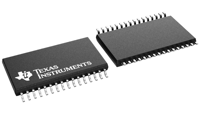
封装信息
| 封装 | 引脚 TSSOP (DA) | 32 |
| 工作温度范围 (°C) -40 to 85 |
| 包装数量 | 包装 46 | TUBE |
THS10082 的特性
- Simultaneous Sampling of Two Single-Ended Signals or One Differential Signal
- Integrated 16-Word FIFO
- Signal-to-Noise and Distortion Ratio: 59 dB at fI = 2 MHz
- Differential Nonlinearity Error: ±1 LSB
- Integral Nonlinearity Error: ±1 LSB
- Auto-Scan Mode for Two Inputs
- 3-V or 5-V Digital Interface Compatible
- Low Power: 216 mW Max
- 5-V Analog Single Supply Operation
- Internal Voltage References ...50 PPM/°C and ±5% Accuracy
- Parallel uC/DSP Interface
- APPLICATIONS
- Radar Applications
- Communications
- Control Applications
- High-Speed DSP Front-End
- Automotive Applications
THS10082 的说明
The THS10082 is a CMOS, low-power, 10-bit, 8 MSPS analog-to-digital converter (ADC). The speed, resolution, bandwidth, and single-supply operation are suited for applications in radar, imaging, high-speed acquisition, and communications. A multistage pipelined architecture with output error correction logic provides for no missing codes over the full operating temperature range. Internal control registers allow for programming the ADC into the desired mode. The THS10082 consists of two analog inputs, which are sampled simultaneously. These inputs can be selected individually and configured to single-ended or differential inputs. An integrated 16 word deep FIFO allows the storage of data in order to take the load off of the processor connected to the ADC. Internal reference voltages for the ADC (1.5 V and 3.5 V) are provided.
An external reference can also be chosen to suit the dc accuracy and temperature drift requirements of the application. Two different conversion modes can be selected. In the single conversion mode, a single and simultaneous conversion can be initiated by using the single conversion start signal (CONVST). The conversion clock in the single conversion mode is generated internally using a clock oscillator circuit. In the continuous conversion mode, an external clock signal is applied to the CONV_CLK input of the THS10082. The internal clock oscillator is switched off in the continuous conversion mode.
The THS10082C is characterized for operation from 0°C to 70°C, and the THS10082I is characterized for operation from –40°C to 85°C.
