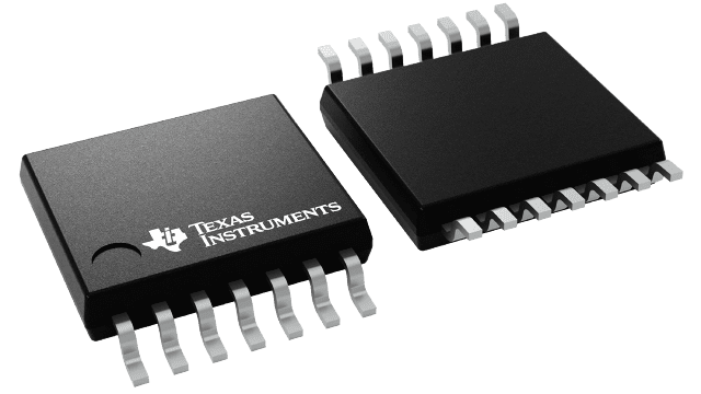
封装信息
| 封装 | 引脚 TSSOP (PW) | 14 |
| 工作温度范围 (°C) -40 to 85 |
| 包装数量 | 包装 2,000 | LARGE T&R |
SN74CBT3126 的特性
- Standard ’126-Type Pinout (D, DB, DGV, and PW Packages)
- 5-
 Switch Connection Between Two Ports
 - TTL-Compatible Input Levels
- Latch-Up Performance Exceeds 250 mA Per JESD 17
SN74CBT3126 的说明
The SN74CBT3126 quadruple FET bus switch features independent line switches. Each switch is disabled when the associated output-enable (OE) input is low.
To ensure the high-impedance state during power up or power down, OE should be tied to GND through a pullup resistor; the minimum value of the resistor is determined by the current-sourcing capability of the driver.