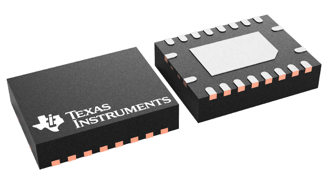
封装信息
| 封装 | 引脚 VQFN (RGY) | 20 |
| 工作温度范围 (°C) -40 to 85 |
| 包装数量 | 包装 3,000 | LARGE T&R |
SN74AUCH244 的特性
- Optimized for 1.8-V Operation and is 3.6-V I/O Tolerant to Support Mixed-Mode Signal Operation
- Ioff Supports Partial-Power-Down Mode Operation
- Sub 1-V Operable
- Max tpd of 1.9 ns at 1.8 V
- Low Power Consumption, 20-µA Max ICC
- ±8-mA Output Drive at 1.8 V
- Bus Hold on Data Inputs Eliminates the Need for External Pullup/Pulldown Resistors
- Latch-Up Performance Exceeds 100 mA Per JESD 78, Class II
- ESD Protection Exceeds JESD 22
- 2000-V Human-Body Model (A114-A)
- 200-V Machine Model (A115-A)
- 1000-V Charged-Device Model (C101)
SN74AUCH244 的说明
This octal buffer/driver is operational at 0.8-V to 2.7-V VCC, but is designed specifically for 1.65-V to 1.95-V VCC operation.
The SN74AUCH244 is organized as two 4-bit line drivers with separate output-enable (OE)\ inputs. When OE\ is low, the device passes data from the A inputs to the Y outputs. When OE\ is high, the outputs are in the high-impedance state.
To ensure the high-impedance state during power up or power down, OE\ should be tied to VCC through a pullup resistor; the minimum value of the resistor is determined by the current-sinking capability of the driver.
Active bus-hold circuitry holds unused or undriven inputs at a valid logic state. Use of pullup or pulldown resistors with the bus-hold circuitry is not recommended.
This device is fully specified for partial-power-down applications using Ioff. The Ioff circuitry disables the outputs, preventing damaging current backflow through the device when it is powered down.