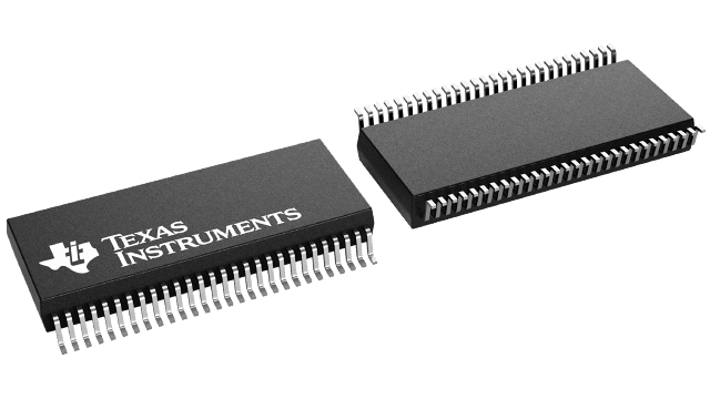
封装信息
| 封装 | 引脚 SSOP (DL) | 56 |
| 工作温度范围 (°C) -40 to 85 |
| 包装数量 | 包装 20 | TUBE |
SN74ABT162827A 的特性
- Members of the Texas Instruments Widebus™ Family
- Output Ports Have Equivalent 25-
 Series Resistors, So No External Resistors Are Required
 - High-Impedance State During Power Up and Power Down
- Typical VOLP (Output Ground Bounce)
< 1 V at VCC= 5 V, TA = 25°C - Distributed VCC and GND Pin Minimizes High-Speed Switching Noise
- Ioff and Power-Up 3-State Support Hot Insertion
- Flow-Through Architecture Optimizes PCB Layout
- Latch-Up Performance Exceeds 500 mA Per JEDEC Standard JESD-17
- ESD Protection Exceeds JESD 22
- 2000-V Human-Body Model (A114-A)
- 200-V Machine Model (A115-A)
Widebus is a trademark of Texas Instruments.
SN74ABT162827A 的说明
The ’ABT162827A devices are noninverting 20-bit buffers composed of two 10-bit buffers with separate output-enable signals. For either 10-bit buffer, the two output-enable (1OE1\ and 1OE2\, or 2OE1\ and 2OE2\) inputs must both be low for the corresponding Y outputs to be active. If either output-enable input is high, the outputs of that 10-bit buffer are in the high-impedance state.
The outputs, which are designed to source or sink up to 12 mA, include equivalent 25- series resistors to reduce overshoot and undershoot.
These devices are fully specified for hot-insertion applications using Ioff and power-up 3-state. The Ioff circuitry disables the outputs, preventing damaging current backflow through the devices when they are powered down. The power-up 3-state circuitry places the outputs in the high-impedance state during power up and power down, which prevents driver conflict.
To ensure the high-impedance state during power up or power down, OE\ shall be tied to VCC through a pullup resistor; the minimum value of the resistor is determined by the current-sinking capability of the driver.
