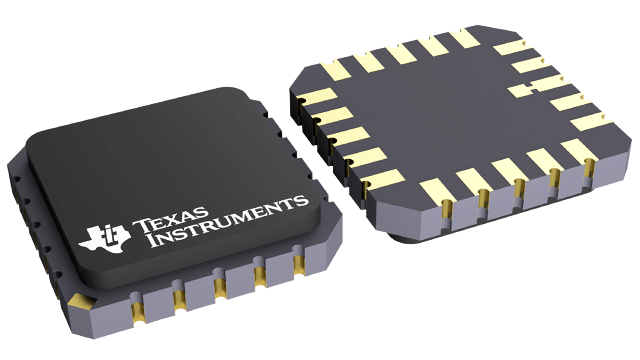
封装信息
| 封装 | 引脚 LCCC (FK) | 20 |
| 工作温度范围 (°C) -55 to 125 |
| 包装数量 | 包装 55 | TUBE |
SN54LS273 的特性
- Contains Eight Flip-Flops With Single-Rail Outputs
- Buffered Clock and Direct Clear Inputs
- Individual Data Input to Each Flip-Flop
- Applications Include:
- Buffer/Storage Registers
- Shift Registers
- Pattern Generators
SN54LS273 的说明
These monolithic, positive-edge-triggered flip-flops utilize TTL circuitry to implement D-type flip-flop logic with a direct clear input.
Information at the D inputs meeting the setup time requirements is transferred to the Q outputs on the positive-going edge of the clock pulse. Clock triggering occurs at a particular voltage level and is not directly related to the transition time of the positive-going pulse. When the clock input is at either the high or low level, the D input signal has no effect at the output.
These flip-flops are guaranteed to respond to clock frequencies ranging form 0 to 30 megahertz while maximum clock frequency is typically 40 megahertz. Typical power dissipation is 39 milliwatts per flip-flop for the ´273 and 10 milliwatts for the ´LS273.