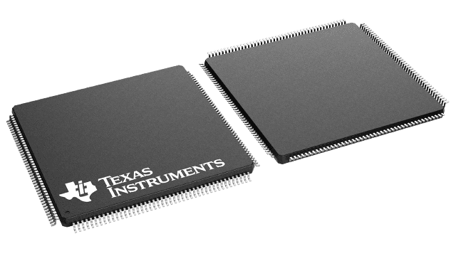
封装信息
| 封装 | 引脚 LQFP (PGF) | 176 |
| 工作温度范围 (°C) -55 to 125 |
| 包装数量 | 包装 40 | JEDEC TRAY (10+1) |
SM320F2812-EP 的特性
- Controlled Baseline
- One Assembly/Test/Fabrication Site
- Extended Temperature Performance of –55°C to 125°C
- Enhanced Diminishing Manufacturing Sources (DMS) Support
- Enhanced Product-Change Notification
- Qualification Pedigree(1)
- High-Performance Static CMOS Technology
- 150 MHz (6.67-ns Cycle Time)
- Low-Power (1.8-V Core @135 MHz, 1.9-V Core @150 MHz, 3.3-V I/O) Design
- JTAG Boundary Scan Support(2)
- High-Performance 32-Bit CPU (320C28x)
- 16 × 16 and 32 × 32 MAC Operations
- 16 × 16 Dual MAC
- Harvard Bus Architecture
- Atomic Operations
- Fast Interrupt Response and Processing
- Unified Memory Programming Model
- 4M Linear Program/Data Address Reach
- Code-Efficient (in C/C++ and Assembly)
- 320F24x/LF240x Processor Source Code Compatible
- On-Chip Memory
- Flash Devices: Up to 128K × 16 Flash
(Four 8K × 16 and Six 16K × 16 Sectors) - ROM Devices: Up to 128K × 16 ROM
- 1K × 16 OTP ROM
- L0 and L1: 2 Blocks of 4K × 16 Each Single-Access RAM (SARAM)
- H0: 1 Block of 8K × 16 SARAM
- M0 and M1: 2 Blocks of 1K × 16 Each SARAM
- Flash Devices: Up to 128K × 16 Flash
- Boot ROM (4K × 16)
- With Software Boot Modes
- Standard Math Tables
- External Interface (2812)
- Over 1M × 16 Total Memory
- Programmable Wait States
- Programmable Read/Write Strobe Timing
- Three Individual Chip Selects
- Clock and System Control
- Dynamic PLL Ratio Changes Supported
- On-Chip Oscillator
- Watchdog Timer Module
- Three External Interrupts
- Peripheral Interrupt Expansion (PIE) Block
That Supports 45 Peripheral Interrupts - Three 32-Bit CPU-Timers
- 128-Bit Security Key/Lock
- Protects Flash/ROM/OTP and L0/L1 SARAM
- Prevents Firmware Reverse Engineering
- Motor Control Peripherals
- Two Event Managers (EVA, EVB)
- Compatible to 240xA Devices
- Serial Port Peripherals
- Serial Peripheral Interface (SPI)
- Two Serial Communications Interfaces (SCIs), Standard UART
- Enhanced Controller Area Network (eCAN)
- Multichannel Buffered Serial Port (McBSP)
- 12-Bit ADC, 16 Channels
- 2 × 8 Channel Input Multiplexer
- Two Sample-and-Hold
- Single/Simultaneous Conversions
- Fast Conversion Rate: 80 ns/12.5 MSPS
- Up to 56 General Purpose I/O (GPIO) Pins
- Advanced Emulation Features
- Analysis and Breakpoint Functions
- Real-Time Debug via Hardware
- Development Tools Include
- ANSI C/C++ Compiler/Assembler/Linker
- Code Composer Studio™ IDE
- DSP/BIOS™
- Low-Power Modes and Power Savings
- IDLE, STANDBY, HALT Modes Supported
- Disable Individual Peripheral Clocks
- Package Options
- 179-Ball MicroStar BGA™ (GHH), (2812)
- 176-Pin Low-Profile Quad Flatpack (LQFP) (PGF) (2812)
TMS320C24x, Code Composer Studio, DSP/BIOS, and MicroStar BGA are trademarks of Texas Instruments.
(1) Component qualification in accordance with JEDEC and industry standards to ensure reliable operation over an extended temperature range.
This includes, but is not limited to, Highly Accelerated Stress Test (HAST) or biased 85/85, temperature cycle, autoclave or unbiased HAST,
electromigration, bond intermetallic life, and mold compound life. Such qualification testing should not be viewed as justifying use of this
component beyond specified performance and environmental limits.
(2) IEEE Standard 1149.1-1990, IEEE Standard Test-Access Port
SM320F2812-EP 的说明
The SM320F2810-EP, SM320F2811-EP, SM320F2812-EP, SM320C2810-EP, SM320C2811-EP, and SM320C2812-EP devices, members of the TMS320C28x™ DSP generation, are highly integrated, high-performance solutions for demanding control applications. The functional blocks and the memory maps are described in Section 3, Functional Overview.
Throughout this document, SM320F2810-EP, SM320F2811-EP, and SM320F2812-EP are abbreviated as F2810, F2811, and F2812, respectively. F281x denotes all three Flash devices. SM320C2810-EP, SM320C2811-EP, and SM320C2812-EP are abbreviated as C2810, C2811, and C2812, respectively. C281x denotes all three ROM devices. 2810 denotes both F2810 and C2810 devices; 2811 denotes both F2811 and C2811 devices; and 2812 denotes both F2812 and C2812 devices.
