SCDS247B October 2008 – February 2016 TS12A44513 , TS12A44514 , TS12A44515
PRODUCTION DATA.
1 Features
- 2-V to 12-V Single-Supply Operation
- Specified ON-State Resistance:
- 15-Ω Maximum With 12-V Supply
- 20-Ω Maximum With 5-V Supply
- 50-Ω Maximum With 3.3-V Supply
- ΔRON Matching
- 2.5-Ω (Max) at 12 V
- 3-Ω (Max) at 5 V
- 3.5-Ω (Max) at 3.3 V
- Specified Low OFF-Leakage Currents:
- 1 nA at 25°C
- 10 nA at 85°C
- Specified Low ON-Leakage Currents:
- 1 nA at 25°C
- 10 nA at 85°C
- Low Charge Injection: 11.5 pC (12-V Supply)
- Fast Switching Speed:
tON = 80 ns, tOFF = 50 ns (12-V Supply) - Break-Before-Make Operation (tON > tOFF)
- TTL/CMOS-Logic Compatible With 5-V Supply
- Available in 14-Pin TSSOP Package or 14-Pin SOIC Package
2 Applications
- Data Acquisition Systems
- Communication Circuits
- Signal Routing
- Computer Peripherals
3 Description
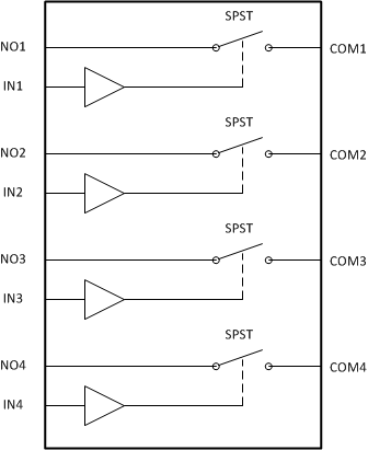
The TS12A44513, TS12A44514, and TS12A44515 devices have four bidirectional single-pole single-throw (SPST) single-supply CMOS analog switches. The TS12A44513 has two normally closed (NC) switches and two normally open (NO) switches, the TS12A44514 has four NO switches, and the TS12A44515 has four NC switches.
These CMOS switches may operate continuously with a single supply from 2 V to 12 V and can handle rail-to-rail analog signals. The OFF-leakage current maximum is only 1 nA at 25°C or 10 nA at 85°C.
When using a 5-V supply, all digital inputs have 0.8-V to 2.4-V logic thresholds, ensuring TTL/CMOS-logic compatibility.
Device Information(1)
| PART NUMBER | PACKAGE | BODY SIZE (NOM) |
|---|---|---|
| TS12A44513, TS12A44514, TS12A44515 | TSSOP (14) | 5.00 mm x 4.4 mm |
| SOIC (14) | 8.65 mm x 3.91 mm |
- For all available packages, see the orderable addendum at the end of the datasheet.
Simplified Schematic

4 Revision History
Changes from A Revision (November 2014) to B Revision
- Changed VCC min value from 0 to 2 in Recommended Operating Conditions tableGo
- Added Supply column back into all Electrical Characteristics tablesGo
Changes from * Revision (October 2008) to A Revision
- Added Pin Configuration and Functions section, ESD Ratings table, Feature Description section, Device Functional Modes, Application and Implementation section, Power Supply Recommendations section, Layout section, Device and Documentation Support section, and Mechanical, Packaging, and Orderable Information section Go