SWCS046U March 2010 – October 2014 TPS65910
PRODUCTION DATA.
- 1Device Overview
- 2Revision History
- 3 Device Comparison
- 4Terminal Configuration and Functions
-
5Specifications
- 5.1 Absolute Maximum Ratings
- 5.2 Handling Ratings
- 5.3 Recommended Operating Conditions
- 5.4 Thermal Resistance Characteristics for RSL Package
- 5.5 I/O Pullup and Pulldown Characteristics
- 5.6 Digital I/O Voltage Electrical Characteristics
- 5.7 I2C Interface and Control Signals
- 5.8 Power Consumption
- 5.9 Power References and Thresholds
- 5.10 Thermal Monitoring and Shutdown
- 5.11 32-kHz RTC Clock
- 5.12 Backup Battery Charger
- 5.13 VRTC LDO
- 5.14 VIO SMPS
- 5.15 VDD1 SMPS
- 5.16 VDD2 SMPS
- 5.17 VDD3 SMPS
- 5.18 VDIG1 and VDIG2 LDO
- 5.19 VAUX33 and VMMC LDO
- 5.20 VAUX1 and VAUX2 LDO
- 5.21 VDAC and VPLL LDO
- 5.22
Timing and Switching Characteristics
- 5.22.1 Switch-On/-Off Sequences and Timing
- 5.22.2
Power Control Timing
- 5.22.2.1 Device Turn-On/Off With Rising/Falling Input Voltage
- 5.22.2.2 Device State Control Through PWRON Signal
- 5.22.2.3 Device SLEEP State Control
- 5.22.2.4 Power Supplies State Control Through the SCLSR_EN1 and SDASR_EN2 Signals
- 5.22.2.5 VDD1 and VDD2 Voltage Control Through SCLSR_EN1 and SDASR_EN2 Signals
- 5.22.2.6 SMPS Switching Synchronization
-
6Detailed Description
- 6.1 Power Reference
- 6.2 Power Sources
- 6.3 Embedded Power Controller
- 6.4 32-kHz RTC Clock
- 6.5 RTC
- 6.6 Backup Battery Management
- 6.7 Backup Registers
- 6.8 I2C Interface
- 6.9 Thermal Monitoring and Shutdown
- 6.10 Interrupts
- 6.11 Package Description
- 6.12 Functional Registers
- 7Device and Documentation Support
- 8Mechanical Packaging and Orderable Information
1 Device Overview
1.1 Features
- Embedded Power Controller
- Two Efficient Step-Down DC-DC Converters for Processor Cores
- One Efficient Step-Down DC-DC Converter for I/O Power
- One Efficient Step-Up 5-V DC-DC Converter
- SmartReflex™ Compliant Dynamic Voltage Management for Processor Cores
- 8 LDO Voltage Regulators and One Real-Time Clock (RTC) LDO (Internal Purpose)
- One High-Speed I2C Interface for General-Purpose Control Commands (CTL-I2C)
- One High-Speed I2C Interface for SmartReflex Class 3 Control and Command (SR-I2C)
- Two Enable Signals Multiplexed with SR-I2C, Configurable to Control any Supply State and Processor Cores Supply Voltage
- Thermal Shutdown Protection and Hot-Die Detection
- An RTC Resource With:
- Oscillator for 32.768-kHz Crystal or 32-kHz Built-in RC Oscillator
- Date, Time, and Calendar
- Alarm Capability
- One Configurable GPIO
- DC-DC Switching Synchronization Through Internal or External 3-MHz Clock
1.2 Applications
- Portable and Handheld Systems
- Industrial Systems
1.3 Description
The TPS65910 device is an integrated power-management IC available in 48-QFN package and dedicated to applications powered by one Li-Ion or Li-Ion polymer battery cell or 3-series Ni-MH cells, or by a 5-V input; it requires multiple power rails. The device provides three step-down converters, one step-up converter, and eight LDOs and is designed to support the specific power requirements of OMAP-based applications.
Two of the step-down converters provide power for dual processor cores and are controllable by a dedicated class-3 SmartReflex interface for optimum power savings. The third converter provides power for the I/Os and memory in the system.
The device includes eight general-purpose LDOs providing a wide range of voltage and current capabilities. The LDOs are fully controllable by the I2C interface. The use of the LDOs is flexible; they are intended to be used as follows: Two LDOs are designated to power the PLL and video DAC supply rails on the OMAP-based processors, four general-purpose auxiliary LDOs are available to provide power to other devices in the system, and two LDOs are provided to power DDR memory supplies in applications requiring these memories.
In addition to the power resources, the device contains an embedded power controller (EPC) to manage the power sequencing requirements of the OMAP systems and an RTC.
1.4 Functional Block Diagram
Figure 1-1 shows the top-level diagram of the device.
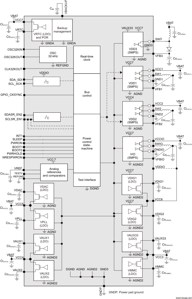 Figure 1-1 48-QFN Top-Level Diagram