SWCS046U March 2010 – October 2014 TPS65910
PRODUCTION DATA.
- 1Device Overview
- 2Revision History
- 3 Device Comparison
- 4Terminal Configuration and Functions
-
5Specifications
- 5.1 Absolute Maximum Ratings
- 5.2 Handling Ratings
- 5.3 Recommended Operating Conditions
- 5.4 Thermal Resistance Characteristics for RSL Package
- 5.5 I/O Pullup and Pulldown Characteristics
- 5.6 Digital I/O Voltage Electrical Characteristics
- 5.7 I2C Interface and Control Signals
- 5.8 Power Consumption
- 5.9 Power References and Thresholds
- 5.10 Thermal Monitoring and Shutdown
- 5.11 32-kHz RTC Clock
- 5.12 Backup Battery Charger
- 5.13 VRTC LDO
- 5.14 VIO SMPS
- 5.15 VDD1 SMPS
- 5.16 VDD2 SMPS
- 5.17 VDD3 SMPS
- 5.18 VDIG1 and VDIG2 LDO
- 5.19 VAUX33 and VMMC LDO
- 5.20 VAUX1 and VAUX2 LDO
- 5.21 VDAC and VPLL LDO
- 5.22
Timing and Switching Characteristics
- 5.22.1 Switch-On/-Off Sequences and Timing
- 5.22.2
Power Control Timing
- 5.22.2.1 Device Turn-On/Off With Rising/Falling Input Voltage
- 5.22.2.2 Device State Control Through PWRON Signal
- 5.22.2.3 Device SLEEP State Control
- 5.22.2.4 Power Supplies State Control Through the SCLSR_EN1 and SDASR_EN2 Signals
- 5.22.2.5 VDD1 and VDD2 Voltage Control Through SCLSR_EN1 and SDASR_EN2 Signals
- 5.22.2.6 SMPS Switching Synchronization
-
6Detailed Description
- 6.1 Power Reference
- 6.2 Power Sources
- 6.3 Embedded Power Controller
- 6.4 32-kHz RTC Clock
- 6.5 RTC
- 6.6 Backup Battery Management
- 6.7 Backup Registers
- 6.8 I2C Interface
- 6.9 Thermal Monitoring and Shutdown
- 6.10 Interrupts
- 6.11 Package Description
- 6.12 Functional Registers
- 7Device and Documentation Support
- 8Mechanical Packaging and Orderable Information
4 Terminal Configuration and Functions
Figure 4-1 shows the pin assignments.
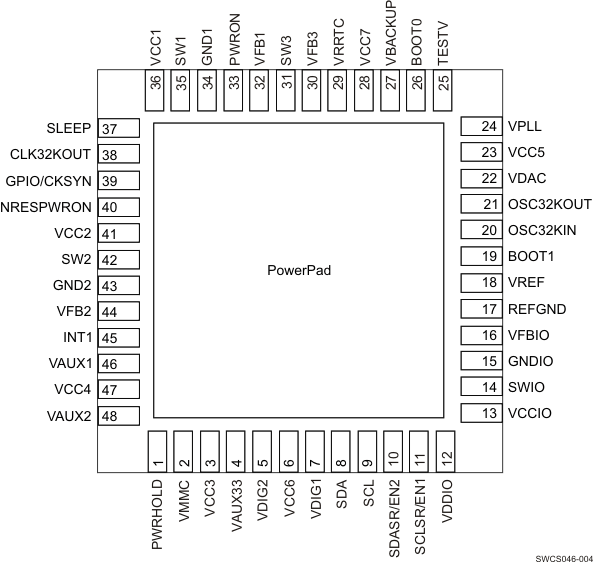 Figure 4-1 48-QFN Top-View Pin Assignment
4.1 Signal Descriptions
Table 4-1 Signal Descriptions
| NAME | QFN PIN | SUPPLIES | TYPE | I/O | DESCRIPTION | PU/PD |
|---|---|---|---|---|---|---|
| VDDIO | VDDIO/DGND | Power | I | Digital I/Os supply | No | |
| SDA_SDI | VDDIO/DGND | Digital | I/O | I2C bidirectional data signal/serial peripheral interface data input (multiplexed) | External PU | |
| SCL_SCK | VDDIO/DGND | Digital | I/O | I2C bidirectional clock signal/serial peripheral interface Clock Input (multiplexed) | External PU | |
| SDASR_EN2 | VDDIO/DGND | Digital | I/O | I2C SmartReflex bidirectional data signal/enable of supplies (multiplexed) | External PU | |
| SCLSR_EN1 | VDDIO/DGND | Digital | I/O | I2C SmartReflex bidirectional clock signal/enable of supplies (multiplexed) | External PU | |
| SLEEP | VDDIO/DGND | Digital | I | Active-sleep state transition control signal | Programmable PD (default active) |
|
| GPIO_CKSYNC | VDDIO/DGND | Digital | I/O | Configurable general-purpose I/O or DC-DCs synchronization clock input signal | Programmable PD (default active) |
|
| PWRHOLD | VRTC/DGND | Digital | I | Switch-on/-off control signal | Programmable PD (default active) |
|
| PWRON | VBAT/DGND | Digital | I | External switch-on control (ON button) | Programmable PU (default active) |
|
| NRESPWRON | VDDIO/DGND | Digital | O | Power off reset | PD active during device OFF state | |
| INT1 | VDDIO/DGND | Digital | O | Interrupt flag | No | |
| BOOT0 | VRTC/DGND | Digital | I | Power-up sequence selection | Programmable PD (default active) |
|
| BOOT1 | VRTC/DGND | Digital | I | Power-up sequence selection | Programmable PD (default active) |
|
| CLK32KOUT | VDDIO/DGND | Digital | O | 32-kHz clock output | PD disable in ACTIVE or SLEEP state | |
| OSC32KIN | VRTC/REFGND | Analog | I | 32-kHz crystal oscillator | No | |
| OSC32KOUT | VRTC/REFGND | Analog | I | 32-kHz crystal oscillator | No | |
| VREF | VCC7/REFGND | Analog | O | Bandgap voltage | No | |
| REFGND | REFGND | Analog | I/O | Reference ground | No | |
| TESTV | VCC7/AGND | Analog | O | Analog test output (DFT) | No | |
| VBACKUP | VBACKUP/AGND | Power | I | Backup battery input (short to VCC5 if not used) | No | |
| VCC1 | VCC1/GND1 | Power | I | VDD1 DC-DC power input | No | |
| GND1 | VCC1/GND1 | Power | I/O | VDD1 DC-DC power ground | No | |
| SW1 | VCC1/GND1 | Power | O | VDD1 DC-DC switched output | No | |
| VFB1 | VCC7/AGND | Analog | I | VDD1 feedback voltage | PD | |
| VCC2 | VCC2/GND2 | Power | I | VDD2 DC-DC power input | No | |
| GND2 | VCC2/GND2 | Power | I/O | VDD2 DC-DC power ground | No | |
| SW2 | VCC2/GND2 | Power | O | VDD2 DC-DC switched output | No | |
| VFB2 | VCC4/AGND2 | Analog | I | VDD2 DC-DC feedback voltage | PD | |
| VCCIO | VCCIO/GNDIO | Power | I | VIO DC-DC power input | No | |
| GNDIO | VCCIO/GNDIO | Power | I/O | VIO DC-DC power ground | No | |
| SWIO | VCCIO/GNDIO | Power | O | VIO DC-DC switched output | No | |
| VFBIO | VCC7/AGND | Analog | I | VIO feedback voltage | PD | |
| VCC3 | VCC3/AGND2 | Power | I | VMMC VAUX33 power input | No | |
| VMMC | VCC3/REFGND | Power | O | LDO regulator output | PD | |
| VAUX33 | VCC3/REFGND | Power | O | LDO regulator output, VDD3 internal regulated supply | PD | |
| VCC4 | VCC4/AGND2 | Power | I | VAUX1, VAUX2 power input | No | |
| VAUX1 | VCC4/REFGND | Power | O | LDO regulator output | PD | |
| VAUX2 | VCC4/REFGND | Power | O | LDO regulator output | PD | |
| VCC5 | VCC5/AGND | Power | I | VDAC, VPLL power input | No | |
| VDAC | VCC5/REFGND | Power | O | LDO regulator output | PD | |
| VPLL | VCC5/REFGND | Power | O | LDO regulator output | PD | |
| VRTC | VCC7/REFGND | Power | O | LDO regulator output | PD | |
| VCC6 | VCC6/AGND2 | Power | I | VDIG1, VDIG2 power input | No | |
| VDIG1 | VCC6/REFGND | Power | O | LDO regulator output | No | |
| VDIG2 | VCC6/REFGND | Power | O | LDO regulator output | No | |
| VCC7 | VCC7/REFGND | Power | I | VRTC power input, VDD3 internal and analog references supply | No | |
| VFB3 | VCC7/AGND | Analog | I | VDD3 feedback voltage | No | |
| SW3 | VCC7/GND3 | Power | O | VDD3 DC-DC switched output | No | |
| GND3 | Power PAD | AGND | Power | I/O | VDD3 DC-DC power ground | No |
| AGND | Power PAD | AGND | Power | I/O | Analog ground | No |
| AGND2 | Power PAD | AGND | Power | I/O | Analog ground | No |
| DGND | Power PAD | DGND | Power | I/O | Digital ground | No |