SLVS845G March 2009 – August 2014 TPS54362-Q1
PRODUCTION DATA.
- 1 Features
- 2 Applications
- 3 Description
- 4 Revision History
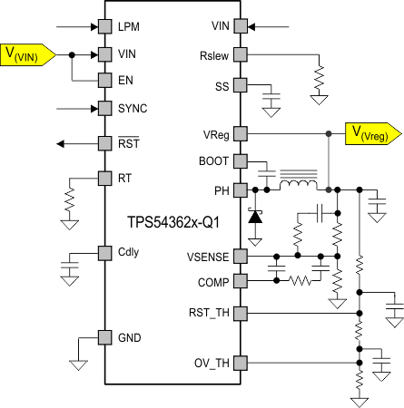
- 5 Pin Configuration and Functions
- 6 Specifications
-
7 Detailed Description
- 7.1 Overview
- 7.2 Functional Block Diagram
- 7.3
Feature Description
- 7.3.1 Input Voltage
- 7.3.2 Function Mode
- 7.3.3 Output Voltage V(VReg)
- 7.3.4 Oscillator Frequency (RT)
- 7.3.5 Synchronization (SYNC)
- 7.3.6 Enable or Shutdown (EN)
- 7.3.7 Reset Delay (Cdly)
- 7.3.8 Reset Pin (RST)
- 7.3.9 Boost Capacitor (BOOT)
- 7.3.10 Soft Start (SS)
- 7.3.11 Short-Circuit Protection
- 7.3.12 Overcurrent Protection
- 7.3.13 Slew Rate Control (Rslew)
- 7.3.14 Thermal Shutdown
- 7.3.15 Regulation Voltage (VSENSE)
- 7.3.16 RESET Threshold (RST_TH)
- 7.3.17 Overvoltage Supervisor for V(VReg) (OV_TH)
- 7.3.18 Noise Filter on RST_TH and OV_TH Pins
- 7.3.19 Output Tolerances Based on Modes of Operation
- 7.3.20 Load Regulation and Line Regulation in Hysteretic Mode
- 7.3.21 Internal Undervoltage Lockout (UVLO)
- 7.3.22 Loop-Control Frequency Compensation
- 7.3.23 Bode Plot of Converter Gain
- 7.4 Device Functional Modes
-
8 Application and Implementation
- 8.1 Application Information
- 8.2
Typical Application
- 8.2.1 Design Requirements
- 8.2.2
Detailed Design Procedure
- 8.2.2.1 Selecting the Switching Frequency
- 8.2.2.2 Output Inductor Selection (LO)
- 8.2.2.3 Output Capacitor (CO)
- 8.2.2.4 Flyback Schottky Diode
- 8.2.2.5 Input Capacitor, C(I)
- 8.2.2.6 Output Voltage and Feedback Resistor Selection
- 8.2.2.7 Overvoltage Resistor Selection
- 8.2.2.8 Reset-Threshold Resistor Selection
- 8.2.2.9 Low-Power Mode Threshold
- 8.2.2.10 Undervoltage Threshold for Low-Power Mode and Load-Transient Operation
- 8.2.2.11 Soft-Start Capacitor
- 8.2.2.12 Bootstrap Capacitor Selection
- 8.2.2.13 Guidelines for Compensation Components
- 8.2.2.14 Compensation
- 8.2.3 Application Curves
- 9 Power Supply Recommendations
- 10Layout
- 11Device and Documentation Support
- 12Mechanical, Packaging, and Orderable Information
1 Features
- Qualified for Automotive Applications
- AEC-Q100 Qualified With the Following Results:
- Withstands Transients up to 60 V With an Operating Range of 3.6 V to 48 V
- Asynchronous Switch-Mode Regulator With External Components (L and C), Load Current up to 3 A (max.)
- 0.8 V ± 1.5% Voltage Reference
- 200-kHz to 2.2-MHz Switching Frequency
- High-Voltage-Tolerant Enable Input for ON/OFF State
- Soft Start on Enable Cycle
- Slew-Rate Control on Internal Power Switch
- External Clock Input for Synchronization
- Pulse-Skip Mode (PFM) During Light Output Loads With Quiescent Current = 65 μA Typical (LPM Operation)
- External Compensation for Wide-Bandwidth Error Amplifier
- Internal Undervoltage Lockout, UVLO
- Programmable Reset Power-On Delay
- Reset-Function Filter Time for Fast Negative Transients
- Programmable Overvoltage Output Monitoring
- Programmable Undervoltage Output Monitoring, Issuance of Reset if Output Falls Below Threshold
- Thermal Shutdown During Excessive Power Dissipation
- Switch Current-Limit Protection
- Short-Circuit and Overcurrent Protection of FET
- Junction Temperature Range: –40°C to 150°C
- 20-Pin HTSSOP PowerPAD™ Package
- Qualified for Automotive Applications
2 Applications
- Automotive Telematics
- Navigation Systems
- In-Dash Instrumentation
- Battery-Powered Applications
3 Description
The TPS54362-Q1 device is a step-down switch-mode power supply with a low-power mode and a programmable voltage supervisor. Integrated input voltage-line feed-forward topology improves line transient regulation of the voltage-mode buck regulator. The regulator has a cycle-by-cycle current limit. Pulse-skip mode operation under no load reduces the supply current to 65 μA. Using the enable pin reduces the supply shutdown current to 1 μA.
An open-drain reset signal indicates when the nominal output drops below the threshold set by an external resistor-divider network. A soft-start capacitor controls the output voltage start-up ramp. The device activates an internal undervoltage shutdown when the input supply ramps down to 2.6 V.
Frequency foldback operation protects the device during an overload conditions on the output. The device also has thermal shutdown protection due to excessive power dissipation.
The B-revision has an improved leakage current parameter, and improved discharged function while in disable mode.
Device Information(1)
| PART NUMBER | PACKAGE | BODY SIZE (NOM) |
|---|---|---|
| TPS54362-Q1 | HTSSOP (20) | 6.50 mm × 4.40 mm |
- For all available packages, see the orderable addendum at the end of the datasheet.
4 Revision History
Changes from F Revision (May 2014) to G Revision
- Added AEC-Q100 qualification features to the Features section Go
- Added product improvements for B-revision silicon under the Product Description sectionGo
- Increased the max output voltage value for the SS pin in the Absolute Maximum Ratings table Go
- Changed column in Thermal Table from TPS54362A, to TPS54362xGo
- Changed the IIKG row in Elec Chara Table from TPS54362A-Q1 to A-revision and TPS54362B-Q1 to B-revisionGo
- Increased the maximum Ilkg value for both B-revision test conditions in the Electrical Characteristics table Go
- Changed in CAUTION: TPS54362A-Q1 to TPS54362Ax-Q1 and deleted TPS54362B-Q1Go
- Changed in Soft-Start Capacitor paragraph TPS54362A-Q1 to TPS54362Ax-Q1 and deleted TPS54362B-Q1Go
- Changed Power Supply Recommendations section: TPS54362A-Q1 to TPS54362Ax-Q1 and deleted TPS54362B-Q1Go
Changes from E Revision (May 2013) to F Revision
- Changed all text, tables and graphics to the new data sheet template. Go
- Changed pinout drawingGo
- Changed parameter symbols for JEDEC compliance throughout the data sheet Go
- Added a row for the Rslew pin to the Absolute Maximum Ratings tableGo
- Changed symbol for thermal resistance from θ to Rθ in the Thermal Information table Go
- Added Ilkg parameters for EN pin on TPS54362B-Q1 deviceGo
- Revised Figure 22Go
- Changed value of R4 in Output Voltage and Feedback Resistor Selection sectionGo
- Changed several values in the Overvoltage Resistor Selection sectionGo
- Changed several values in the Reset-Threshold Resistor Selection sectionGo
- Changed the voltage value in the Undervoltage Threshold for Low-Power Mode and Load-Transient Operation sectionGo
- Added the TPS54362B-Q1 part number to the text of the Soft-Start Capacitor sectionGo
- Changed calculated values for loop compensation componentsGo
Changes from D Revision (October 2011) to E Revision
- Removed TPS54362-Q1 and TPS54362 from data sheet; added -Q1 to TPS54362A part numbers.Go
- Removed Ordering Information table; see Package Option Addendum for ordering information.Go
- Removed items 3 and 4 from the Soft Start (SS) section, also removed the sentence: Item 3 and item 4 are not applicable for TPS54362A-Q1.Go
- Removed the following sentence from the Soft-Start Capacitor section: Equation 4 has to be satisfied in addition to the other conditions stated in the soft start section of this document (not applicable for TPS54362A-Q1).Go