SLVS845G March 2009 – August 2014 TPS54362-Q1
PRODUCTION DATA.
- 1 Features
- 2 Applications
- 3 Description
- 4 Revision History
- 5 Pin Configuration and Functions
- 6 Specifications
-
7 Detailed Description
- 7.1 Overview
- 7.2 Functional Block Diagram
- 7.3
Feature Description
- 7.3.1 Input Voltage
- 7.3.2 Function Mode
- 7.3.3 Output Voltage V(VReg)
- 7.3.4 Oscillator Frequency (RT)
- 7.3.5 Synchronization (SYNC)
- 7.3.6 Enable or Shutdown (EN)
- 7.3.7 Reset Delay (Cdly)
- 7.3.8 Reset Pin (RST)
- 7.3.9 Boost Capacitor (BOOT)
- 7.3.10 Soft Start (SS)
- 7.3.11 Short-Circuit Protection
- 7.3.12 Overcurrent Protection
- 7.3.13 Slew Rate Control (Rslew)
- 7.3.14 Thermal Shutdown
- 7.3.15 Regulation Voltage (VSENSE)
- 7.3.16 RESET Threshold (RST_TH)
- 7.3.17 Overvoltage Supervisor for V(VReg) (OV_TH)
- 7.3.18 Noise Filter on RST_TH and OV_TH Pins
- 7.3.19 Output Tolerances Based on Modes of Operation
- 7.3.20 Load Regulation and Line Regulation in Hysteretic Mode
- 7.3.21 Internal Undervoltage Lockout (UVLO)
- 7.3.22 Loop-Control Frequency Compensation
- 7.3.23 Bode Plot of Converter Gain
- 7.4 Device Functional Modes
-
8 Application and Implementation
- 8.1 Application Information
- 8.2
Typical Application
- 8.2.1 Design Requirements
- 8.2.2
Detailed Design Procedure
- 8.2.2.1 Selecting the Switching Frequency
- 8.2.2.2 Output Inductor Selection (LO)
- 8.2.2.3 Output Capacitor (CO)
- 8.2.2.4 Flyback Schottky Diode
- 8.2.2.5 Input Capacitor, C(I)
- 8.2.2.6 Output Voltage and Feedback Resistor Selection
- 8.2.2.7 Overvoltage Resistor Selection
- 8.2.2.8 Reset-Threshold Resistor Selection
- 8.2.2.9 Low-Power Mode Threshold
- 8.2.2.10 Undervoltage Threshold for Low-Power Mode and Load-Transient Operation
- 8.2.2.11 Soft-Start Capacitor
- 8.2.2.12 Bootstrap Capacitor Selection
- 8.2.2.13 Guidelines for Compensation Components
- 8.2.2.14 Compensation
- 8.2.3 Application Curves
- 9 Power Supply Recommendations
- 10Layout
- 11Device and Documentation Support
- 12Mechanical, Packaging, and Orderable Information
8 Application and Implementation
8.1 Application Information
This section is a starting point, with theoretical representation of the values used for the application. Improving the performance of the device may require further optimization of the component values.
8.2 Typical Application
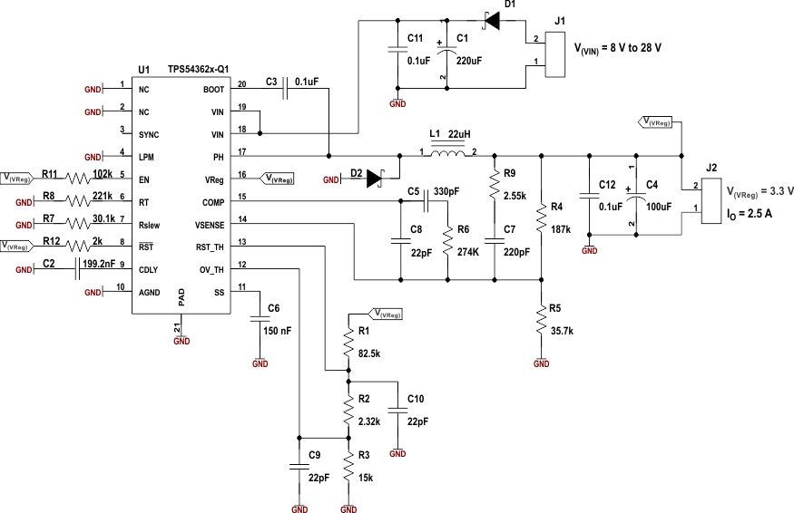
8.2.1 Design Requirements
For this design example, use the parameters listed in Table 3.
Table 3. Design Parameters
| DESIGN PARAMETER | EXAMPLE VALUE |
|---|---|
| Input voltage, VI | 8 V to 28 V |
| Output voltage, VO | 5 V ± 2% |
| Maximum output current, IO-max | 3 A |
| Transient response 0.25-A to 2.25-A load step | ΔVO = 5% |
| Reset threshold | 92% of output voltage |
| Overvoltage threshold | 106% of output voltage |
| Undervoltage threshold | 95% of output voltage |
8.2.2 Detailed Design Procedure
8.2.2.1 Selecting the Switching Frequency
The user selects the switching frequency based on the minimum on-time of the internal power switch, the maximum input voltage, the minimum output voltage, and the frequency-shift limitations. Use Equation 19 to find the maximum frequency for the regulator. Determine the value of the resistor to connect to the RT pin to set this frequency from Figure 13.
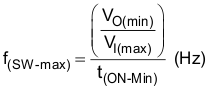
where
- f(SW-max) = 770 kHz
- t(ON-Min) = 150 ns from the Electrical Characteristics table
Because the oscillator can vary 10%, decrease the frequency by 10%. Further, to keep the switching frequency outside the AM band, one can select f(sw) as 400 kHz (500 kHz in the application example).
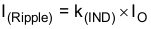
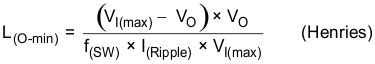
8.2.2.2 Output Inductor Selection (LO)
Calculate the minimum inductor value using Equation 21.
k(IND) is the coefficient that represents the amount of inductor ripple current relative to the maximum output current. Calculate the ripple using Equation 20.
The output capacitor filters the inductor ripple current, and so the typical range of this ripple current is in the range calculated with k(IND) = 0.2 to 0.3, depending on the ESR and the ripple-current rating of the output capacitor. The minimum inductor value calculated is 14.5 μH; choose an inductor ≈ 22 μH.
where
- I(Ripple) = 0.2 × 2.5 = 0.5 A (peak-to-peak)
Calculate inductor L(O):
where
- f(SW) is the regulator switching frequency
- I(Ripple) = Allowable ripple current in the inductor, typically 20% of maximum IO
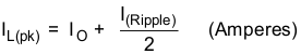
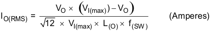
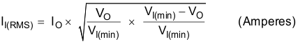
The RMS (root-mean-square) and peak current flowing in the inductor is:
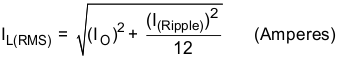
Inductor peak current:
8.2.2.3 Output Capacitor (CO)
The selection of the output capacitor determines several parameters in the operation of the converter, the modulator pole, voltage droop on the output capacitor, and the output ripple.
During a load step from no load to full load or changes in the input voltage, the output capacitor must hold up the output voltage above a certain level for a specified time and not issue a reset, until the main regulator control loop responds to the change. Equation 25 determines the minimum output capacitance required to allow sufficient droop on the output voltage without issuing a reset.
The capacitance value determines the modulator pole and the rolloff frequency due to the LC output filter double pole – Equation 9.
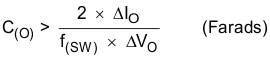
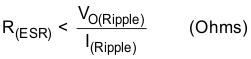
The output ripple voltage is a product of the output capacitor ESR and ripple current – Equation 27.
Using Equation 24, the minimum capacitance needed to maintain the desired output voltage during a high-to-low load transition and prevent overshoot is 157 μF.
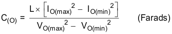
where
- IO(max) is the maximum output current
- IO(min) is the minimum output current
- VO(max) is maximum tolerance of regulated output voltage
- VO(min) is the minimum tolerance of regulated output voltage
The calculation of minimum capacitance needed for transient load response, using Equation 25, yields 53 μF.
The calculation of minimum capacitance needed for output voltage ripple specification, using Equation 26, yields 1.18 μF.
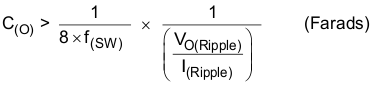
The most critical condition based on the foregoing calculations indicates that the output capacitance must be a minimum of 157 μF to keep the output voltage in regulation during load transients.
Factoring in additional capacitance de-ratings for temperature, aging, and dc bias yields a value of 220 μF. Equation 27 calculates the ESR required to meet the ripple-voltage tolerance of the system, but for system stability the ESR should not exceed 100 mΩ.
Maximum ESR of the out capacitor based on output ripple voltage specification is:
Output capacitor root-mean-square (rms) ripple current. This is to prevent excess heating or failure due to high ripple currents. This parameter is sometimes specified by the manufacturers.
8.2.2.4 Flyback Schottky Diode
The TPS54362-Q1 device requires an external Schottky diode connected between the PH pin and the power ground termination. The absolute voltage at the PH pin should not go beyond the values mentioned in Absolute Maximum Ratings. The Schottky diode conducts the output current during the off state of the internal power switch. This Schottky diode must have a reverse breakdown higher than the maximum input voltage of the application. The low forward voltage of a Schottky diode makes it ideal for this situation. Select the Schottky diode based on the appropriate power rating, which factors in the dc conduction losses and the ac losses due to the high switching frequencies; Equation 29 determines the power requirement.
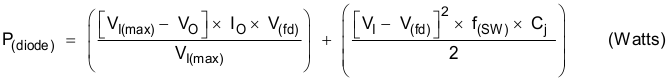
where
- VF = forward conducting voltage of Schottky diode
- Cj = junction capacitance of the Schottky diode
The recommended part numbers of the Flyback Schottky diodes are PDS360 and SBR8U60P5.
8.2.2.5 Input Capacitor, C(I)
The requires an input ceramic decoupling capacitor with type X5R or X7R dielectric, and bulk capacitance to minimize input ripple voltage. The dc voltage rating of this input capacitance must be greater than the maximum input voltage. The capacitor must have an input ripple current rating higher than the maximum input ripple current of the converter for the application; Equation 30 determines the ripple current.
The input capacitors for power regulators are chosen to have reasonable capacitance-to-volume ratio and fairly stable over temperature. The value of the input capacitance also determines the input ripple voltage of the regulator, shown by Equation 31.
8.2.2.6 Output Voltage and Feedback Resistor Selection
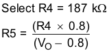
In the design example, the R4 selection is 187 kΩ; using Equation 1, R4 calculates as 35.7 kΩ. To minimize the effect of leakage current on the VSENSE pin, the current flowing through the feedback network should be greater than 5 μA in order to maintain output accuracy. Higher resistor values help improve the converter efficiency at low output currents, but may introduce noise immunity problems.
8.2.2.7 Overvoltage Resistor Selection
Use Equation 6to determine the value of R3 to set the overvoltage threshold at 1.06 × 5.5 V. The total resistor network from the VReg output to ground is approximately 100 kΩ (this is R1 + R2 +R3). The calculated value of R3 is then 15.09 kΩ. Use the nearest standard value, which is 15 kΩ. This pin may require a noise decoupling capacitor to ensure proper operation; the value chosen for this design is 56 pF.
8.2.2.8 Reset-Threshold Resistor Selection
Using Equation 5, calculate the value of R2 + R3, and then knowing R3 from the OV_TH setting, determine R2. The value of R2 + R3 yields 17.39 kΩ, which means R2 is approximately 2.32 kΩ. This sets the reset threshold at 0.92 × 5 V. This pin may require a noise-decoupling capacitor to ensure proper operation; the value chosen for this design is 15 pF. The value determined for R1 is 82.5 kΩ.
8.2.2.9 Low-Power Mode Threshold
To obtain an approximation of the output load current at which the converter is operating in discontinuous mode, use Equation 32. The values used in the equation for minimum and maximum input voltage affect the duty cycle and the overall discontinuous-mode (DCM) load current. With a maximum input voltage of 28 V, the output load current for DCM is 165.8 mA, and for minimum input voltage of 8 V, the DCM-mode load current is 111.7 mA. These are nominal values, calculated without taking into consideration other factors like external component variations with temperature and aging.

where
- IL(DCM) = Output load current at which the converter is operating in discontinuous mode
- IL(LPM) = Output load current at which the converter is operating in low-power mode
- D = Duty cycle
8.2.2.10 Undervoltage Threshold for Low-Power Mode and Load-Transient Operation
Setting the undervoltage threshold above the reset threshold ensures the regulator operates within the specified tolerances during output load transients of low load to high load and during discontinuous conduction mode. Using Equation 4, determine the typical voltage threshold.
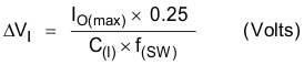
8.2.2.11 Soft-Start Capacitor
The soft-start capacitor determines the minimum time to reach the desired output voltage during a power-up cycle. This time is important when a load requires a controlled voltage-slew rate. Soft starting helps to limit the current draw from the input voltage supply line. This design requires a 4.7-nF capacitor to meet the soft-start criteria. If the buck converter starts up with output shorted to ground, the circuit requires a TPS54362-Q1 device and a minimum 150-nF C(SS).
8.2.2.12 Bootstrap Capacitor Selection
Connect a 0.1-μF ceramic capacitor between the PH and BOOT pins for the converter to operate and regulate the desired output voltage. TI recommends using a capacitor with X5R or better-grade dielectric material, and a voltage rating on this capacitor of at least 25 V to allow for derating.
8.2.2.13 Guidelines for Compensation Components
Make the two zeroes close to the double pole (LC), for example, f(z1) ≈ f(z2) ≈ 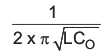 .
.
- Make the first zero below the filter double pole (approximately 50% to 75% of f(LC)).
- Make the second zero at the filter double pole (f(LC)).
Make the two poles above the crossover frequency f(c),
- Make the first pole at the ESR frequency (f(ESR)).
- Make the second pole at 0.5 the switching frequency (0.5 × f(SW)).
Calculate C5 based on placing a zero at 50% to 75% of the output-filter double-pole frequency.
Calculate C8 by placing the first pole at the ESR zero frequency.
Set the second pole at 0.5 times the switching frequency, and also set the second zero at the output-filter double-pole frequency.
8.2.2.14 Compensation
8.2.2.14.1 Calculate the Loop Compensation
DC modulator gain (A(mod)) = 8 / V(ramp)
V(ramp) = 0.8 V
A(mod) (dB) = 20 log (10) = 20 dB
Output filter due to LCO poles and CO ESR zeros from Equation 9 and Equation 10.
f(LC) = 3.4 kHz for LCO = 22 µH, CO = 100 µF
f(ESR) = 15.9 kHz for CO = 100 µF, ESR = 100 mΩ
Choose R4 = 187 kΩ.
Calculate the poles and zeros for a type III network using equations Equation 33 to Equation 38.
R5 = 35.7 kΩ (use standard value 35.7 kΩ)
R6 = 276 kΩ (use standard value 274 kΩ)
C5 = 340 pF (use standard value 330 pF)
C8 = 40.6 pF (use standard value 22 pF)
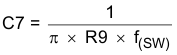
R9 = 2.57 kΩ (use standard value 2.55 kΩ)
C7 = 247 pF (use standard value 220 pF)
Calculate the poles and zeros based on these compensation values, using Equation 15 through Equation 18.
8.2.2.14.2 Power Dissipation
The power dissipation losses applicable for continuous-conduction-mode operation (CCM) are:
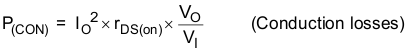


where:
VO = Output voltage
VI = Input voltage
IO = Output current
tr = FET switching rise time (maximum tr = 40 ns)
tf = FET switching fall time
V(drive) = FET gate-drive voltage (typically V(drive) = 6 V and maximum V(drive) = 8 V)
f(sw) = Switching frequency
For a given operating ambient temperature TA
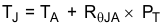
For a given maximum junction temperature TJ-Max = 150°C
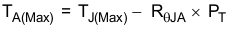
where:
PT = Total power dissipation (watts)
TA = Ambient temperature in °C
TJ = Junction temperature in °C
TA(Max) = Maximum ambient temperature in °C
TJ(Max) = Maximum junction temperature in °C
RθJA = Thermal resistance of package in (°C/W)
Other factors not included in the preceding information which affect the overall efficiency and power losses are:
- Inductor ac and dc losses
- Trace resistance and losses associated with the copper trace routing and connections
- Flyback catch diode
The output current rating for the regulator may require derating for ambient temperatures above 85°C. The derating value depends on the calculated worst-case power dissipation and the thermal management implementation in the application.
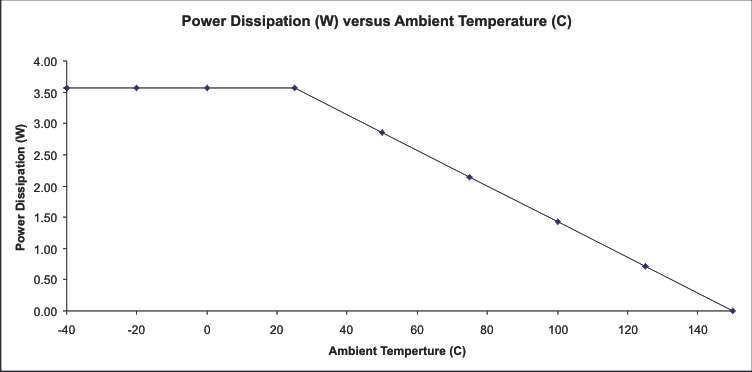 Figure 23. Power Dissipation Derating
8.2.3 Application Curves
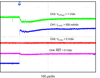
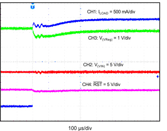
| CH1: IO | CH2: VIN | CH3: Vreg |
| CH4: RST | V(VIN) = 12 V | V(VReg) = 5 V |
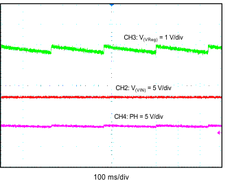
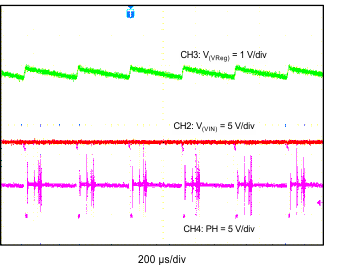
| CH2: VIN | CH3: Vreg | CH4: PH (100 ms/div) |
| V(VIN) = 12 V | V(VReg) = 5 V | CH4 = 1.905 kHz |
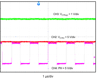
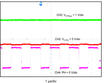
| CH2: VIN | CH3: Vreg | CH4: PH (1 µs/div) |
| V(VIN) = 12 V | V(VReg) = 5 V | CH4 = 519.1 kHz |
| CH1: IO | CH2: VIN | CH3: Vreg |
| CH4: RST | V(VIN) = 12 V | V(VReg) = 5 V |
| CH2: VIN | CH3: Vreg | CH4: PH (200 µs/div) |
| V(VIN) = 12 V | V(VReg) = 5 V | CH4 = 45.7 kHz |
| CH2: VIN | CH3: Vreg | CH4: PH (1 µs/div) |
| V(VIN) = 12 V | V(VReg) = 5 V | CH4 = 523.5 kHz |