-
LM74700-Q1 低 IQ 电池反向保护理想二极管控制器
- 1 特性
- 2 应用
- 3 说明
- 4 Revision History
- 5 Pin Configuration and Functions
- 6 Specifications
- 7 Typical Characteristics
- 8 Parameter Measurement Information
- 9 Detailed Description
-
10Application and Implementation
- 10.1 Application Information
- 10.2 OR-ing Application Configuration
- 11Power Supply Recommendations
- 12Layout
- 13Device and Documentation Support
- 14Mechanical, Packaging, and Orderable Information
- 重要声明
LM74700-Q1 低 IQ 电池反向保护理想二极管控制器
1 特性
- 具有符合 AEC-Q100 标准的下列特性
- 器件温度等级 1:
–40°C 至 +125°C 环境工作温度范围 - 器件 HBM ESD 分类等级 2
- 器件 CDM ESD 分类等级 C4B
- 器件温度等级 1:
- 提供功能安全
- 3.2V 至 65V 输入范围(3.9V 启动)
- -65V 反向电压额定值
- 适用于外部 N 沟道 MOSFET 的电荷泵
- 20mV 阳极至阴极正向压降调节
- 使能引脚特性
- 1µA 关断电流(EN = 低电平)
- 80µA 工作静态电流(EN = 高电平)
- 2.3A 峰值栅极关断电流
- 快速响应反向电流阻断:
小于 0.75µs - 采用合适的 TVS 二极管,符合汽车 ISO7637 瞬态要求
- 采用 6 引脚和 8 引脚 SOT-23 封装 2.90mm × 1.60mm
2 应用
- 汽车 ADAS 系统 - 摄像头
- 汽车信息娱乐系统 - 数字仪表盘、主机
- 工业工厂自动化 - PLC
- 企业电源
- 用于冗余电源的有源 ORing
3 说明
LM74700-Q1 是一款符合汽车 AEC Q100 标准的理想二极管控制器,与外部 N 沟道 MOSFET 配合工作,可作为理想二极管整流器利用 20mV 正向压降实现低损耗反向保护。3.2V 至 65V 的宽电源输入范围可实现对众多常用直流总线电压(例如:12V、24V 和 48V 汽车电池系统)的控制。3.2V 输入电压支持适用于汽车系统中严苛的冷启动要求。该器件可耐受低至 –65V 的负电源电压,并提供负载保护。
该器件通过控制 MOSFET 的栅极将正向压降调节至 20mV。该电流调节方案可在反向电流事件中支持平稳关机,并确保零直流反向电流。该器件能够快速 (< 0.75µs) 响应反向电流阻断,因此适用于在 ISO7637 脉冲测试以及电源故障和输入微短路条件下要求保持输出电压的系统。
LM74700-Q1 控制器可提供适用于外部 N 沟道 MOSFET 的电荷泵栅极驱动器。LM74700-Q1 的高电压额定值有助于简化用于汽车 ISO7637 保护的系统设计。当使能引脚处于低电平时,控制器关闭,消耗大约 1µA 的电流。
| 器件型号 | 封装 | 封装尺寸(标称值) |
|---|---|---|
| LM74700-Q1 | SOT-23 (6) | 2.90mm × 1.60mm |
| LM74700-Q1 | SOT-23 (8) | 2.90mm × 1.60mm |
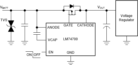 典型应用原理图
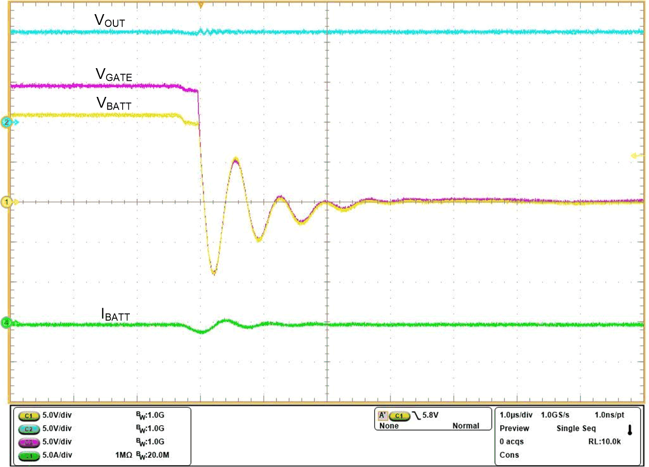 输入短路期间的反向电流阻断
4 Revision History
Changes from Revision F (December 2019) to Revision G (December 2020)
- 更新了整个文档的表、图和交叉参考的编号格式Go
- 向数据表添加了 DDF (SOT-23) 封装Go
- Relaxed VCAP specs in Electrical Characteristics tableGo
Changes from Revision () to Revision ()
Changes from Revision D (January 2019) to Revision E (February 2019)
- 将“预告信息”更改为“量产数据”Go
Changes from Revision C (November 2018) to Revision D (January 2019)
Changes from Revision B (October 2018) to Revision C (November 2018)
Changes from Revision * (October 2017) to Revision A (March 2018)
- 在整个数据表中进行了多处更改Go
5 Pin Configuration and Functions
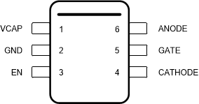 Figure 5-1 DBV Package6-Pin SOT-23Top View
| PIN | I/O(1) | DESCRIPTION | |
|---|---|---|---|
| NO. | NAME | ||
| 1 | VCAP | O | Charge pump output. Connect to external charge pump capacitor |
| 2 | GND | G | Ground pin |
| 3 | EN | I | Enable pin. Can be connected to ANODE for always ON operation |
| 4 | CATHODE | I | Cathode of the diode. Connect to the drain of the external N-channel MOSFET |
| 5 | GATE | O | Gate drive output. Connect to gate of the external N-channel MOSFET |
| 6 | ANODE | I | Anode of the diode and input power. Connect to the source of the external N-channel MOSFET |
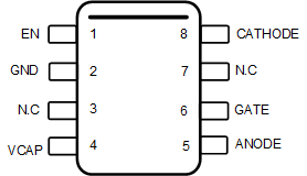 Figure 5-2 DDF Package8-Pin SOT-23Top View
| PIN | I/O(1) | DESCRIPTION | |
|---|---|---|---|
| NO. | NAME | ||
| 1 | EN | I | Enable pin. Can be connected to ANODE for always ON operation |
| 2 | GND | G | Ground pin |
| 3 | N.C | No connection | |
| 4 | VCAP | O | Charge pump output. Connect to external charge pump capacitor |
| 5 | ANODE | I | Anode of the diode and input power. Connect to the source of the external N-channel MOSFET |
| 6 | GATE | O | Gate drive output. Connect to gate of the external N-channel MOSFET |
| 7 | N.C | No connection | |
| 8 | CATHODE | I | Cathode of the diode. Connect to the drain of the external N-channel MOSFET |
6 Specifications
6.1 Absolute Maximum Ratings
| MIN | MAX | UNIT | ||
|---|---|---|---|---|
| Input Pins | ANODE to GND | –65 | 65 | V |
| EN to GND, V(ANODE) > 0 V | –0.3 | 65 | V | |
| EN to GND, V(ANODE) ≤ 0 V | V(ANODE) | (65 + V(ANODE)) | V | |
| Output Pins | GATE to ANODE | –0.3 | 15 | V |
| VCAP to ANODE | –0.3 | 15 | V | |
| Output to Input Pins | CATHODE to ANODE | –5 | 75 | V |
| Operating junction temperature(2) | –40 | 150 | °C | |
| Storage temperature, Tstg | –40 | 150 | °C | |
6.2 ESD Ratings
| VALUE | UNIT | ||||
|---|---|---|---|---|---|
| V(ESD) | Electrostatic discharge | Human body model (HBM), per AEC Q100-002(1) | ±2000 | V | |
| Charged device model (CDM), per AEC Q100-011 | Corner pins (VCAP, EN, ANODE, CATHODE) | ±750 | |||
| Other pins | ±500 | ||||
6.3 Recommended Operating Conditions
| MIN | NOM | MAX | UNIT | ||
|---|---|---|---|---|---|
| Input Pins | ANODE to GND | –60 | 60 | V | |
| CATHODE to GND | 60 | ||||
| EN to GND | –60 | 60 | |||
| Input to Output pins | ANODE to CATHODE | –70 | V | ||
| External capacitance | ANODE | 22 | nF | ||
| CATHODE, VCAP to ANODE | 0.1 | µF | |||
| External MOSFET max VGS rating | GATE to ANODE | 15 | V | ||
| TJ | Operating junction temperature range(2) | –40 | 150 | °C | |
conditions, see Electrical Characteristics.
6.4 Thermal Information
| THERMAL METRIC(1) | LM74700-Q1 | LM74700-Q1 | UNIT | |
|---|---|---|---|---|
| DBV (SOT) | DDF (SOT) | |||
| 6 PINS | 8 PINS | |||
| RθJA | Junction-to-ambient thermal resistance | 189.8 | 133.8 | °C/W |
| RθJC(top) | Junction-to-case (top) thermal resistance | 103.8 | 72.6 | °C/W |
| RθJB | Junction-to-board thermal resistance | 45.8 | 54.5 | °C/W |
| ΨJT | Junction-to-top characterization parameter | 19.4 | 4.6 | °C/W |
| ΨJB | Junction-to-board characterization parameter | 45.5 | 54.2 | °C/W |
6.5 Electrical Characteristics
| PARAMETER | TEST CONDITIONS | MIN | TYP | MAX | UNIT | |
|---|---|---|---|---|---|---|
| VANODE SUPPLY VOLTAGE | ||||||
| V(ANODE) | Operating input voltage | 4 | 60 | V | ||
| V(ANODE POR) | VANODE POR Rising threshold | 3.9 | V | |||
| VANODE POR Falling threshold | 2.2 | 2.8 | 3.1 | V | ||
| V(ANODE POR(Hys)) | VANODE POR Hysteresis | 0.44 | 0.67 | V | ||
| I(SHDN) | Shutdown Supply Current | V(EN) = 0 V | 0.9 | 1.5 | µA | |
| I(Q) | Operating Quiescent Current | 80 | 130 | µA | ||
| ENABLE INPUT | ||||||
| V(EN_IL) | Enable input low threshold | 0.5 | 0.9 | 1.22 | V | |
| V(EN_IH) | Enable input high threshold | 1.06 | 2 | 2.6 | ||
| V(EN_Hys) | Enable Hysteresis | 0.52 | 1.35 | V | ||
| I(EN) | Enable sink current | V(EN) = 12 V | 3 | 5 | µA | |
| VANODE to VCATHODE | ||||||
| V(AK REG) | Regulated Forward V(AK) Threshold | 13 | 20 | 29 | mV | |
| V(AK) | V(AK) threshold for full conduction mode | 34 | 50 | 57 | mV | |
| V(AK REV) | V(AK) threshold for reverse current blocking | –17 | –11 | –2 | mV | |
| Gm | Regulation Error AMP Transconductance(1) | 1200 | 1800 | 3100 | µA/V | |
| GATE DRIVE | ||||||
| I(GATE) | Peak source current | V(ANODE) – V(CATHODE) = 100 mV, V(GATE) – V(ANODE) = 5 V | 3 | 11 | mA | |
| Peak sink current | V(ANODE) – V(CATHODE) = –20 mV, V(GATE) – V(ANODE) = 5 V | 2370 | mA | |||
| Regulation max sink current | V(ANODE) – V(CATHODE) = 0 V, V(GATE) – V(ANODE) = 5 V | 6 | 26 | µA | ||
| RDSON | discharge switch RDSON | V(ANODE) – V(CATHODE) = –20 mV, V(GATE) – V(ANODE) = 100 mV | 0.4 | 2 | Ω | |
| CHARGE PUMP | ||||||
| I(VCAP) | Charge Pump source current (Charge pump on) | V(VCAP) – V(ANODE) = 7 V | 162 | 300 | 600 | µA |
| Charge Pump sink current (Charge pump off) | V(VCAP) – V(ANODE) = 14 V | 5 | 10 | µA | ||
| V(VCAP) – V(ANODE) | Charge pump voltage at V(ANODE) = 3.2 V | I(VCAP) ≤ 30 µA | 8 | V | ||
| Charge pump turn on voltage | 10.8 | 12.1 | 12.9 | V | ||
| Charge pump turn off voltage | 11.6 | 13 | 13.9 | V | ||
| Charge Pump Enable comparator Hysteresis | 0.54 | 0.9 | 1.36 | V | ||
| V(VCAP UVLO) | V(VCAP) – V(ANODE) UV release at rising edge | V(ANODE) – V(CATHODE) = 100 mV | 5.8 | 6.6 | 7.7 | V |
| V(VCAP) – V(ANODE) UV threshold at falling edge | V(ANODE) – V(CATHODE) = 100 mV | 5.11 | 5.68 | 6 | V | |
| CATHODE | ||||||
| I(CATHODE) | CATHODE sink current | V(ANODE) = 12 V, V(ANODE) – V(CATHODE) = –100 mV | 1.7 | 2 | µA | |
| V(ANODE) – V(CATHODE) = –100 mV | 1.2 | 2.2 | µA | |||
| V(ANODE) = –12 V, V(CATHODE) = 12 V | 1.25 | 2.06 | µA | |||
6.6 Switching Characteristics
| PARAMETER | TEST CONDITIONS | MIN | TYP | MAX | UNIT | |
|---|---|---|---|---|---|---|
| ENTDLY | Enable (low to high) to Gate Turn On delay | V(VCAP) > V(VCAP UVLOR) | 75 | 110 | µs | |
| tReverse delay | Reverse voltage detection to Gate Turn Off delay | V(ANODE) – V(CATHODE) = 100 mV to –100 mV | 0.45 | 0.75 | µs | |
| tForward recovery | Forward voltage detection to Gate Turn On delay | V(ANODE) – V(CATHODE) = –100 mV to 700 mV | 1.4 | 2.6 | µs | |
7 Typical Characteristics
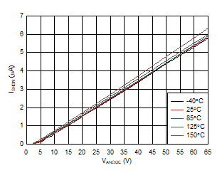 Figure 7-1 Shutdown Supply Current vs Supply Voltage
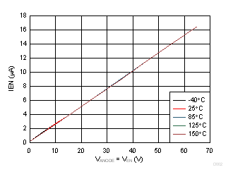 Figure 7-3 Enable Sink Current vs Supply Voltage
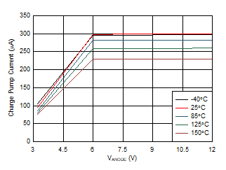 Figure 7-5 Charge Pump Current vs Supply Voltage at VCAP = 6 V
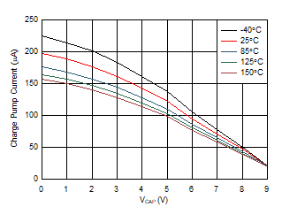 Figure 7-7 Charge Pump V-I Characteristics at VANODE = 3.2 V
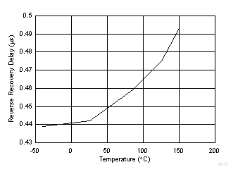 Figure 7-9 Reverse Current Blocking Delay vs Temperature
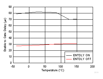 Figure 7-11 Enable to Gate Delay vs Temperature
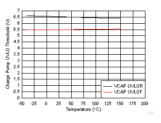 Figure 7-13 Charge Pump UVLO Threshold vs Temperature
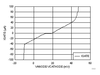 Figure 7-15 Gate
Current vs Forward Voltage Drop
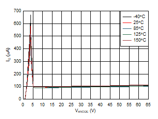 Figure 7-2 Operating Quiescent Current vs Supply Voltage
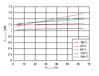 Figure 7-4 CATHODE Sink Current vs Supply Voltage
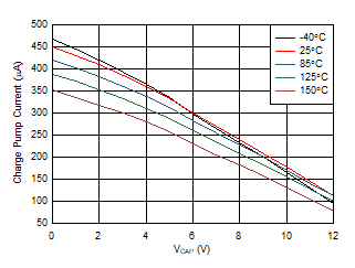 Figure 7-6 Charge Pump V-I Characteristics at VANODE > = 12 V
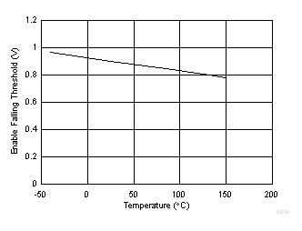 Figure 7-8 Enable Falling Threshold vs Temperature
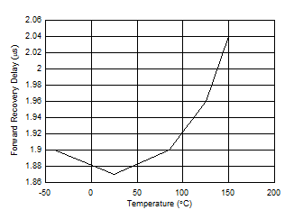 Figure 7-10 Forward Recovery Delay vs Temperature
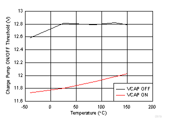 Figure 7-12 Charge Pump ON/OFF Threshold vs Temperature
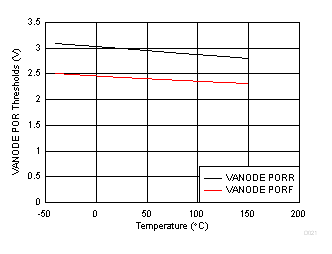 Figure 7-14 VANODE POR Threshold vs Temperature