-
LMK61PD0A2 超低抖动引脚可选振荡器
- 1 特性
- 2 应用
- 3 说明
- 4 修订历史记录
- 5 Device Control
- 6 Pin Configuration and Functions
-
7 Specifications
- 7.1 Absolute Maximum Ratings
- 7.2 ESD Ratings
- 7.3 Recommended Operating Conditions
- 7.4 Thermal Information
- 7.5 Electrical Characteristics - Power Supply
- 7.6 LVPECL Output Characteristics
- 7.7 LVDS Output Characteristics
- 7.8 HCSL Output Characteristics
- 7.9 OE Input Characteristics
- 7.10 OS, FS[1:0] Input Characteristics
- 7.11 Frequency Tolerance Characteristics
- 7.12 Power-On/Reset Characteristics (VDD)
- 7.13 PSRR Characteristics
- 7.14 PLL Clock Output Jitter Characteristics
- 7.15 Additional Reliability and Qualification
- 7.16 Typical Performance Characteristics
- 8 Parameter Measurement Information
- 9 Detailed Description
- 10Application and Implementation
- 11Power Supply Recommendations
- 12Layout
- 13器件和文档支持
- 14机械、封装和可订购信息
- 重要声明
LMK61PD0A2 超低抖动引脚可选振荡器
1 特性
2 应用
- 晶体振荡器、表面声波 (SAW) 振荡器或芯片振荡器的高性能替换产品
- 开关、路由器、网卡、基带装置 (BBU)、服务器、存储/SAN
- 测试和测量
- 医疗成像
- 现场可编程门阵列 (FPGA),处理器连接
3 说明
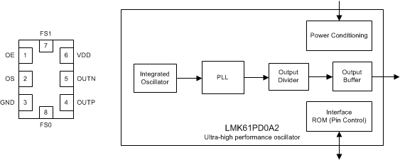
LMK61PD0A2 是一款超低抖动的 PLLatinumTM 引脚可选振荡器。该振荡器可生成通用基准时钟。 该器件在出厂前进行了预编程,可支持七种不同基准时钟频率。相应频率可通过将每个 FS[1:0] 配置为 VDD、GND 或 NC(无连接)进行选择。 输出格式可通过将操作系统 (OS) 的引脚配置为 VDD、GND 或 NC 进行选择,三种配置方式分别对应格式 LVPECL、LVDS 以及 HCSL。 内部电源调节功能提供出色的电源纹波抑制 (PSRR),降低了供电网络的成本和复杂性。 该器件由单个 3.3V ± 5% 电源供电。
器件信息(1)
| 部件号 | 封装 | 封装尺寸(标称值) |
|---|---|---|
| LMK61PD0A2 | 8 引脚 QFM (SIA) | 7.0mm x 5.0mm |
- 要了解所有可用封装,请见数据表末尾的可订购产品附录。
引脚分布和简化框图
5 Device Control
Table 1. Output Frequency Mapping for FS[1:0] Selection
| FS1 | FS0 | OUT FREQUENCY (MHz) | RELEVANT STANDARDS |
| 0 | 0 | 100 | PCI Express |
| 0 | NC | 312.5 | 10 Gbps Ethernet |
| 0 | 1 | 125 | 1 Gbps Ethernet |
| NC | 0 | 106.25 | Fiber Channel |
| NC | NC | 156.25 | 10 Gbps Ethernet |
| NC | 1 | 212.5 | Fiber Channel |
| 1 | 0 | 62.5 | 1 Gbps Ethernet |
| 1 | NC | Reserved | n/a |
| 1 | 1 | Reserved | n/a |
Table 2. Output Type Mapping for OS, OE Selection
| OS | OE | OUTPUT TYPE |
| X | 0 | Disabled (PLL functional) |
| 0 | 1 | LVPECL |
| NC | 1 | LVDS |
| 1 | 1 | HCSL |
6 Pin Configuration and Functions
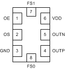
Table 3. Pin Functions
| PIN | I/O | DESCRIPTION | |
|---|---|---|---|
| NAME | NO. | ||
| POWER | |||
| GND | 3 | Ground | Device Ground. |
| VDD | 6 | Analog | 3.3 V Power Supply. |
| OUTPUT BLOCK | |||
| OUTP, OUTN | 4, 5 | Universal | Differential Output Pair (LVPECL, LVDS or HCSL). |
| DIGITAL CONTROL / INTERFACES | |||
| FS[1:0] | 7, 8 | LVCMOS | Output Frequency Select. Refer toTable 1. |
| OE | 1 | LVCMOS | Output Enable (internal pullup). Refer toTable 2. |
| OS | 3 | LVCMOS | Output Type Select. Refer toTable 2. |
7 Specifications
7.1 Absolute Maximum Ratings
over operating free-air temperature range (unless otherwise noted)(1)| MIN | MAX | UNIT | ||
|---|---|---|---|---|
| VDD | Device Supply Voltage | -0.3 | 3.6 | V |
| VIN | Output Voltage Range for Logic Inputs | -0.3 | VDD + 0.3 | V |
| VOUT | Output Voltage Range for Clock Outputs | -0.3 | VDD + 0.3 | V |
| TJ | Junction Temperature | 150 | °C | |
| TSTG | Storage Temperature | -40 | 125 | °C |
7.2 ESD Ratings
| VALUE | UNIT | |||
|---|---|---|---|---|
| V(ESD) | Electrostatic discharge | Human-body model (HBM), per ANSI/ESDA/JEDEC JS-001(1) | ±4000 | V |
| Charged-device model (CDM), per JEDEC specification JESD22-C101(2) | ±1500 | |||
7.3 Recommended Operating Conditions
over operating free-air temperature range (unless otherwise noted)| MIN | NOM | MAX | UNIT | ||
|---|---|---|---|---|---|
| VDD | Device Supply Voltage | 3.135 | 3.3 | 3.465 | V |
| TA | Ambient Temperature | -40 | 25 | 85 | °C |
| TJ | Junction Temperature | 125 | °C | ||
| tRAMP | VDD Power-Up Ramp Time | 0.1 | 100 | ms | |
7.4 Thermal Information
| THERMAL METRIC(1) | LMK61PD0A2 (2) (3) (4) | UNIT | |||
|---|---|---|---|---|---|
| QFM (SIA) | |||||
| 8 PINS | |||||
| Airflow (LFM) 0 | Airflow (LFM) 200 | Airflow (LFM) 400 | |||
| RθJA | Junction-to-ambient thermal resistance | 54 | 44 | 41.2 | °C/W |
| RθJC(top) | Junction-to-case (top) thermal resistance | 34 | n/a | n/a | |
| RθJB | Junction-to-board thermal resistance | 36.7 | n/a | n/a | |
| ψJT | Junction-to-top characterization parameter | 11.2 | 16.9 | 21.9 | |
| ψJB | Junction-to-board characterization parameter | 36.7 | 37.8 | 38.9 | |
| RθJC(bot) | Junction-to-case (bottom) thermal resistance | n/a | n/a | n/a | |
7.5 Electrical Characteristics - Power Supply(1)
VDD = 3.3 V ± 5%, TA = -40C to 85°C| PARAMETER | TEST CONDITIONS | MIN | TYP | MAX | UNIT | |
|---|---|---|---|---|---|---|
| IDD | Device Current Consumption | LVPECL(2) | 162 | 208 | mA | |
| LVDS | 152 | 196 | ||||
| HCSL | 155 | 196 | ||||
| IDD-PD | Device Current Consumption when output is disabled | OE = GND | 136 | |||
7.6 LVPECL Output Characteristics(1)
VDD = 3.3 V ± 5%, TA = -40C to 85°C| PARAMETER | TEST CONDITIONS | MIN | TYP | MAX | UNIT | |
|---|---|---|---|---|---|---|
| fOUT | Output Frequency(2) | 62.5 | 312.5 | MHz | ||
| VOD | Output Voltage Swing (VOH - VOL)(2) |
700 | 800 | 1200 | mV | |
| VOUT, DIFF, PP | Differential Output Peak-to-Peak Swing | 2 x |VOD| | V | |||
| VOS | Output Common Mode Voltage | VDD – 1.55 | V | |||
| tR / tF | Output Rise/Fall Time (20% to 80%)(3) | 120 | 200 | ps | ||
| PN-Floor | Output Phase Noise Floor (fOFFSET > 10 MHz) | 156.25 MHz | -165 | dBc/Hz | ||
| ODC | Output Duty Cycle(3) | 45% | 55% | |||
7.7 LVDS Output Characteristics(1)
VDD = 3.3 V ± 5%, TA = -40°C to 85°C| PARAMETER | TEST CONDITIONS | MIN | TYP | MAX | UNIT | |
|---|---|---|---|---|---|---|
| fOUT | Output Frequency(1) | 62.5 | 312.5 | MHz | ||
| VOD | Output Voltage Swing (VOH - VOL)(1) |
300 | 390 | 480 | mV | |
| VOUT, DIFF, PP | Differential Output Peak-to-Peak Swing | 2 x |VOD| | V | |||
| VOS | Output Common Mode Voltage | 1.2 | V | |||
| tR / tF | Output Rise/Fall Time (20% to 80%)(2) | 150 | 250 | ps | ||
| PN-Floor | Output Phase Noise Floor (fOFFSET > 10 MHz) | 156.25 MHz | -162 | dBc/Hz | ||
| ODC | Output Duty Cycle(2) | 45% | 55% | |||
| ROUT | Differential Output Impedance | 125 | Ohm | |||
7.8 HCSL Output Characteristics(1)
VDD = 3.3 V ± 5%, TA = -40°C to 85°C| PARAMETER | TEST CONDITIONS | MIN | TYP | MAX | UNIT | |
|---|---|---|---|---|---|---|
| fOUT | Output Frequency | 62.5 | 312.5 | MHz | ||
| VOH | Output High Voltage | 600 | 850 | mV | ||
| VOL | Output Low Voltage | -100 | 100 | mV | ||
| VCROSS | Absolute Crossing Voltage(2)(3) | 250 | 475 | mV | ||
| VCROSS-DELTA | Variation of VCROSS(2)(3) | 0 | 140 | mV | ||
| dV/dt | Slew Rate(4) | 0.8 | 2 | V/ns | ||
| PN-Floor | Output Phase Noise Floor (fOFFSET > 10 MHz) | 100 MHz | -164 | dBc/Hz | ||
| ODC | Output Duty Cycle(4) | 45% | 55% | |||
7.9 OE Input Characteristics
VDD = 3.3 V ± 5%, TA = -40°C to 85°C| PARAMETER | TEST CONDITIONS | MIN | TYP | MAX | UNIT | |
|---|---|---|---|---|---|---|
| VIH | Input High Voltage | 1.4 | V | |||
| VIL | Input Low Voltage | 0.6 | V | |||
| IIH | Input High Current | VIH = VDD | -40 | 40 | uA | |
| IIL | Input Low Current | VIL = GND | -40 | 40 | uA | |
| CIN | Input Capacitance | 2 | pF | |||
7.10 OS, FS[1:0] Input Characteristics
VDD = 3.3 V ± 5%, TA = -40°C to 85°C| PARAMETER | TEST CONDITIONS | MIN | TYP | MAX | UNIT | |
|---|---|---|---|---|---|---|
| VIH | Input High Voltage | 1.4 | V | |||
| VIL | Input Low Voltage | 0.4 | V | |||
| IIH | Input High Current | VIH = VDD | -40 | 40 | uA | |
| IIL | Input Low Current | VIL = GND | -40 | 40 | uA | |
| CIN | Input Capacitance | 2 | pF | |||
7.11 Frequency Tolerance Characteristics(1)
VDD = 3.3 V ± 5%, TA = -40°C to 85°C| PARAMETER | TEST CONDITIONS | MIN | TYP | MAX | UNIT | |
|---|---|---|---|---|---|---|
| fT | Total Frequency Tolerance | All output formats, frequency bands and device junction temperature up to 125°C; includes initial freq tolerance, temperature & supply voltage variation, solder reflow and aging (10 years) | -50 | 50 | ppm | |
7.12 Power-On/Reset Characteristics (VDD)
VDD = 3.3 V ± 5%, TA = -40°C to 85°C| PARAMETER | TEST CONDITIONS | MIN | TYP | MAX | UNIT | |
|---|---|---|---|---|---|---|
| VTHRESH | Threshold Voltage(1) | 2.72 | 2.95 | V | ||
| VDROOP | Allowable Voltage Droop(2) | 0.1 | V | |||
| tSTARTUP | Startup Time (1) | Time elapsed from VDD at 3.135 V to output enabled | 10 | ms | ||
| tOE-EN | Output enable time(2) | Time elapsed from OE at VIH to output enabled | 50 | us | ||
| tOE-DIS | Output disable time(2) | Time elapsed from OE at VIL to output disabled | 50 | us | ||
7.13 PSRR Characteristics(1)
VDD = 3.3 V, TA = 25°C, FS[1:0] = NC, NC| PARAMETER | TEST CONDITIONS | MIN | TYP | MAX | UNIT | |
|---|---|---|---|---|---|---|
| PSRR | Spurs Induced by 50 mV Power Supply Ripple(2)(3) at 156.25 MHz output, all output types | Sine wave at 50 kHz | -70 | dBc | ||
| Sine wave at 100 kHz | -70 | |||||
| Sine wave at 500 kHz | -70 | |||||
| Sine wave at 1 MHz | -70 | |||||
7.14 PLL Clock Output Jitter Characteristics(1)(3)
VDD = 3.3 V ± 5%, TA = -40°C to 85°C| PARAMETER | TEST CONDITIONS | MIN | TYP | MAX | UNIT | |
|---|---|---|---|---|---|---|
| RJ | RMS Phase Jitter(2)
(12 kHz – 20 MHz) (1 kHz – 5 MHz) |
fOUT ≥ 100 MHz, All output frequencies and output types | 100 | 200 | fs RMS | |
| RJ | RMS Phase Jitter(2)
(12 kHz – 20 MHz) (1 kHz – 5 MHz) |
fOUT = 62.5 MHz, All output frequencies and output types | 200 | 400 | fs RMS | |
7.15 Additional Reliability and Qualification
| PARAMETER | CONDITION / TEST METHOD |
|---|---|
| Mechanical Shock | MIL-STD-202, Method 213 |
| Mechanical Vibration | MIL-STD-202, Method 204 |
| Moisture Sensitivity Level | J-STD-020, MSL3 |
7.16 Typical Performance Characteristics
![LMK61PD0A2 Phase Noise of LVPECL
Differential Output at 156.25 MHz with FS[1:0] = NC, NC, OS = GND LMK61PD0A2 D001_SNAS674.png](/ods/images/ZHCSEB9A/D001_SNAS674.png) Figure 1. Phase Noise of LVPECL Differential Output at 156.25 MHz with FS[1:0] = NC, NC, OS = GND
Figure 1. Phase Noise of LVPECL Differential Output at 156.25 MHz with FS[1:0] = NC, NC, OS = GND
![LMK61PD0A2 Phase Noise of HCSL
Differential Output at 156.25 MHz with FS[1:0] = NC, NC, OS = VDD LMK61PD0A2 D003_SNAS674.png](/ods/images/ZHCSEB9A/D003_SNAS674.png) Figure 3. Phase Noise of HCSL Differential Output at 156.25 MHz with FS[1:0] = NC, NC, OS = VDD
Figure 3. Phase Noise of HCSL Differential Output at 156.25 MHz with FS[1:0] = NC, NC, OS = VDD
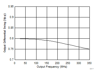 Figure 5. LVDS Differential Output Swing vs Frequency
![LMK61PD0A2 Phase Noise of LVDS
Differential Output at 156.25 MHz with FS[1:0] = NC, NC, OS = NC LMK61PD0A2 D002_SNAS674.png](/ods/images/ZHCSEB9A/D002_SNAS674.png) Figure 2. Phase Noise of LVDS Differential Output at 156.25 MHz with FS[1:0] = NC, NC, OS = NC
Figure 2. Phase Noise of LVDS Differential Output at 156.25 MHz with FS[1:0] = NC, NC, OS = NC
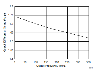 Figure 4. LVPECL Differential Output Swing vs Frequency
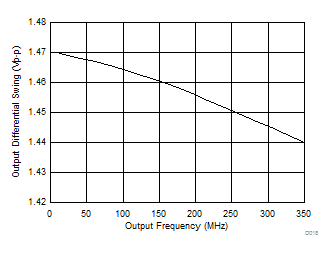 Figure 6. HCSL Differential Output Swing vs Frequency
8 Parameter Measurement Information
8.1 Device Output Configurations
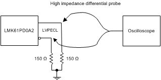 Figure 7. LVPECL Output DC Configuration during Device Test
 Figure 8. LVDS Output DC Configuration during Device Test
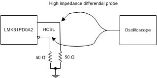 Figure 9. HCSL Output DC Configuration during Device Test
 Figure 10. LVPECL Output AC Configuration during Device Test
 Figure 11. LVDS Output AC Configuration during Device Test
 Figure 12. HCSL Output AC Configuration during Device Test
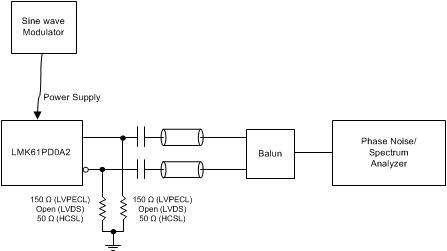 Figure 13. PSRR Test Setup
 Figure 14. Differential Output Voltage and Rise/Fall Time
9 Detailed Description
9.1 Overview
The LMK61PD0A2 is a pin selectable oscillator that generates commonly used reference clocks, greater than 100 MHz, with less than 200 fs, rms max random jitter.
9.2 Functional Block Diagram
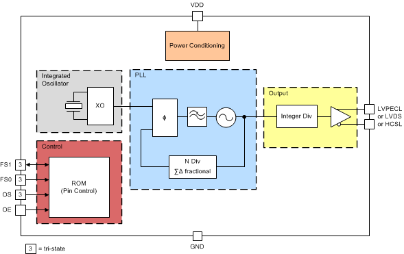
NOTE
Control blocks are compatible with 1.8/2.5/3.3 V I/O voltage levels.
9.3 Feature Description
9.3.1 Device Block-Level Description
The LMK61PD0A2 comprises of an integrated oscillator that includes a 50 MHz crystal, a fractional PLL with integrated VCO. Completing the device is the combination of an integer output divider and a universal differential output buffer. The on-chip ROM contains seven pre-programmed output frequency plans that selects the appropriate settings for the integrated oscillator, PLL blocks and output divider. Table 1 lists the supported output frequency plans that can be selected by pin-strapping FS[1:0] as required. Table 2 lists the supported output types that can be selected by pin-strapping OS and OE as required. The device is powered by on-chip low dropout (LDO) linear voltage regulators and the regulated supply network is partitioned such that the sensitive analog supplies are running from separate LDOs than the digital supplies which use their own LDO. The LDOs provide isolation from any noise in the external power supply rail with a PSRR of better than -70 dBc at 50 kHz to 1 MHz ripple frequencies at 3.3 V device supply.
9.3.2 Device Configuration Control
The LMK61PD0A2 selects an output frequency plan and output type using control pins FS[1:0].
10 Application and Implementation
NOTE
Information in the following applications sections is not part of the TI component specification, and TI does not warrant its accuracy or completeness. TI’s customers are responsible for determining suitability of components for their purposes. Customers should validate and test their design implementation to confirm system functionality.
10.1 Application Information
The LMK61PD0A2 is an ultra-low jitter pin selectable oscillator that can be used to provide reference clocks for high-speed serial links resulting in improved system performance.
10.2 Typical Application
10.2.1 Jitter Considerations in Serdes Systems
Jitter-sensitive applications such as 10 Gbps or 100 Gbps Ethernet, deploy a serial link utilizing a Serializer in the transmit section (TX) and a De-serializer in the receive section (RX). These SERDES blocks are typically embedded in an ASIC or FPGA. Estimating the clock jitter impact on the link budget requires understanding of the TX PLL bandwidth and the RX CDR bandwidth.
As can be seen in Figure 15, the pass band region between the TX low pass cutoff and RX high pass cutoff frequencies is the range over which the reference clock jitter adds without any attenuation to the jitter budget of the link. Outside of these frequencies, the SERDES link will attenuate the reference clock jitter with a 20 dB/dec or even steeper roll-off. Modern ASIC or FPGA designs have some flexibility on deciding the optimal RX CDR bandwidth and TX PLL bandwidth. These bandwidths are typically set based on what is achievable in the ASIC or FPGA process node, without increasing design complexity, and on any jitter tolerance or wander specification that needs to be met, as related to the RX CDR bandwidth.
The overall allowable jitter in a serial link is dictated by IEEE or other relevant standards. For example, IEEE802.3ba states that the maximum transmit jitter (peak-peak) for 10 Gbps Ethernet should be no more than 0.28 * UI and this equates to a 27.1516 ps, p-p for the overall allowable transmit jitter.
The jitter contributing elements are made up of the reference clock, generated potentially from a device like LMK61PD0A2, the transmit medium, transmit driver etc. Only a portion of the overall allowable transmit jitter is allocated to the reference clock, typically 20% or lower. Therefore, the allowable reference clock jitter, for a 20% clock jitter budget, is 5.43 ps, p-p.
Jitter in a reference clock is made up of deterministic jitter (arising from spurious signals due to supply noise or mixing from other outputs or from the reference input) and random jitter (usually due to thermal noise and other uncorrelated noise sources). A typical clock tree in a serial link system consists of clock generators and fanout buffers. The allowable reference clock jitter of 5.43 ps, p-p is needed at the output of the fanout buffer. Modern fanout buffers have low additive random jitter (less than 100 fs, rms) with no substantial contribution to the deterministic jitter. Therefore, the clock generator and fanout buffer contribute to the random jitter while the primary contributor to the deterministic jitter is the clock generator. Rule of thumb, for modern clock generators, is to allocate 25% of allowable reference clock jitter to the deterministic jitter and 75% to the random jitter. This amounts to an allowable deterministic jitter of 1.36 ps, p-p and an allowable random jitter of 4.07 ps, p-p. For serial link systems that need to meet a bit error rate (BER) of 10-12, the allowable random jitter in root-mean-square is 0.29 ps, rms. This is calculated by dividing the p-p jitter by 14 for a BER of 10-12. Accounting for random jitter from the fanout buffer, the random jitter needed from the clock generator is 0.27 ps, rms. This is calculated by the root-mean-square subtraction from the desired jitter at the fanout buffer's output assuming 100 fs, rms of additive jitter from the fanout buffer.
With careful frequency planning techniques, like spur optimization (covered in the Spur Mitigation Techniques section) and on-chip LDOs to suppress supply noise, the LMK61PD0A2 is able to generate clock outputs with deterministic jitter that is below 1 ps, p-p and random jitter that is below 0.2 ps, rms. This gives the serial link system with additional margin on the allowable transmit jitter resulting in a BER better than 10-12.
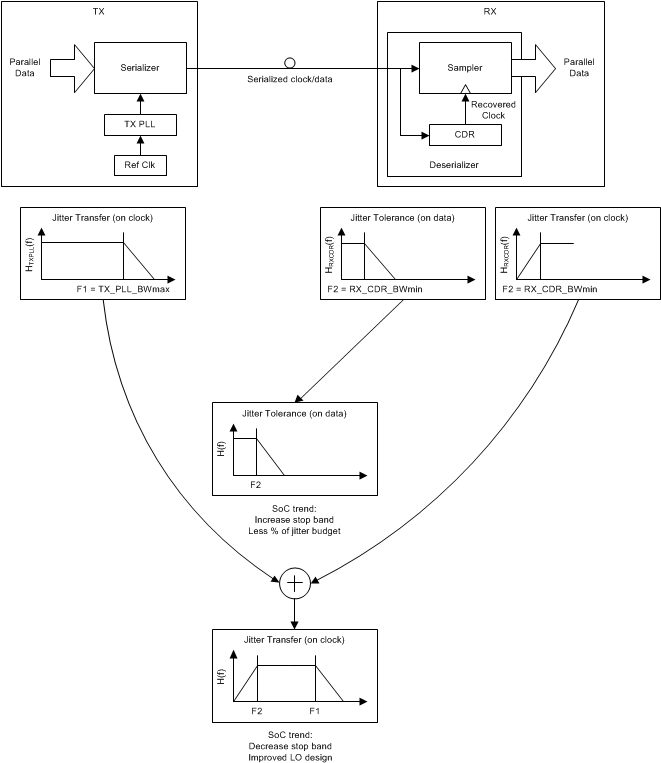 Figure 15. Dependence of Clock Jitter in Serial Links
11 Power Supply Recommendations
For best electrical performance of LMK61PD0A2, it is preferred to utilize a combination of 10 uF, 1 uF and 0.1 uF on its power supply bypass network. It is also recommended to utilize component side mounting of the power supply bypass capacitors and it is best to use 0201 or 0402 body size capacitors to facilitate signal routing. Keep the connections between the bypass capacitors and the power supply on the device as short as possible. Ground the other side of the capacitor using a low impedance connection to the ground plane. Figure 16 shows the layout recommendation for power supply decoupling of LMK61PD0A2.