• Menu
  • Product
  • Email
  • PDF
  • Order now
  • 具有内部 EEPROM 的 LMK61E2 超低抖动可编程振荡器

    • ZHCSE74B September   2015  – February 2017 LMK61E2

      PRODUCTION DATA.  

  • CONTENTS
  • SEARCH
  • 具有内部 EEPROM 的 LMK61E2 超低抖动可编程振荡器
  1. 1 特性
  2. 2 应用
  3. 3 说明
  4. 4 修订历史记录
  5. 5 Pin Configuration and Functions
  6. 6 Specifications
    1. 6.1  Absolute Maximum Ratings
    2. 6.2  ESD Ratings
    3. 6.3  Recommended Operating Conditions
    4. 6.4  Thermal Information
    5. 6.5  Electrical Characteristics - Power Supply
    6. 6.6  LVPECL Output Characteristics
    7. 6.7  LVDS Output Characteristics
    8. 6.8  HCSL Output Characteristics
    9. 6.9  OE Input Characteristics
    10. 6.10 ADD Input Characteristics
    11. 6.11 Frequency Tolerance Characteristics
    12. 6.12 Power-On/Reset Characteristics (VDD)
    13. 6.13 I2C-Compatible Interface Characteristics (SDA, SCL)
    14. 6.14 PSRR Characteristics
    15. 6.15 Other Characteristics
    16. 6.16 PLL Clock Output Jitter Characteristics
    17. 6.17 Typical 156.25-MHz Output Phase Noise Characteristics
    18. 6.18 Typical 161.1328125 MHz Output Phase Noise Characteristics
    19. 6.19 Additional Reliability and Qualification
    20. 6.20 Typical Characteristics
  7. 7 Parameter Measurement Information
    1. 7.1 Device Output Configurations
  8. 8 Detailed Description
    1. 8.1 Overview
    2. 8.2 Functional Block Diagram
    3. 8.3 Feature Description
      1. 8.3.1  Device Block-Level Description
      2. 8.3.2  Device Configuration Control
      3. 8.3.3  Register File Reference Convention
      4. 8.3.4  Configuring the PLL
      5. 8.3.5  Integrated Oscillator
      6. 8.3.6  Reference Doubler
      7. 8.3.7  Phase Frequency Detector
      8. 8.3.8  Feedback Divider (N)
      9. 8.3.9  Fractional Circuitry
      10. 8.3.10 Charge Pump
      11. 8.3.11 Loop Filter
      12. 8.3.12 VCO Calibration
      13. 8.3.13 High-Speed Output Divider
      14. 8.3.14 High-Speed Clock Output
      15. 8.3.15 Device Status
        1. 8.3.15.1 Loss of Lock
    4. 8.4 Device Functional Modes
      1. 8.4.1 Interface and Control
    5. 8.5 Programming
      1. 8.5.1 I2C Serial Interface
      2. 8.5.2 Block Register Write
      3. 8.5.3 Block Register Read
      4. 8.5.4 Write SRAM
      5. 8.5.5 Write EEPROM
      6. 8.5.6 Read SRAM
      7. 8.5.7 Read EEPROM
    6. 8.6 EEPROM Map
    7. 8.7 Register Map
      1. 8.7.1 Register Descriptions
        1. 8.7.1.1  VNDRID_BY1 Register; R0
        2. 8.7.1.2  VNDRID_BY0 Register; R1
        3. 8.7.1.3  PRODID Register; R2
        4. 8.7.1.4  REVID Register; R3
        5. 8.7.1.5  SLAVEADR Register; R8
        6. 8.7.1.6  EEREV Register; R9
        7. 8.7.1.7  DEV_CTL Register; R10
        8. 8.7.1.8  XO_CAPCTRL_BY1 Register; R16
        9. 8.7.1.9  XO_CAPCTRL_BY0 Register; R17
        10. 8.7.1.10 DIFFCTL Register; R21
        11. 8.7.1.11 OUTDIV_BY1 Register; R22
        12. 8.7.1.12 OUTDIV_BY0 Register; R23
        13. 8.7.1.13 PLL_NDIV_BY1 Register; R25
        14. 8.7.1.14 PLL_NDIV_BY0 Register; R26
        15. 8.7.1.15 PLL_FRACNUM_BY2 Register; R27
        16. 8.7.1.16 PLL_FRACNUM_BY1 Register; R28
        17. 8.7.1.17 PLL_FRACNUM_BY0 Register; R29
        18. 8.7.1.18 PLL_FRACDEN_BY2 Register; R30
        19. 8.7.1.19 PLL_FRACDEN_BY1 Register; R31
        20. 8.7.1.20 PLL_FRACDEN_BY0 Register; R32
        21. 8.7.1.21 PLL_MASHCTRL Register; R33
        22. 8.7.1.22 PLL_CTRL0 Register; R34
        23. 8.7.1.23 PLL_CTRL1 Register; R35
        24. 8.7.1.24 PLL_LF_R2 Register; R36
        25. 8.7.1.25 PLL_LF_C1 Register; R37
        26. 8.7.1.26 PLL_LF_R3 Register; R38
        27. 8.7.1.27 PLL_LF_C3 Register; R39
        28. 8.7.1.28 PLL_CALCTRL Register; R42
        29. 8.7.1.29 NVMSCRC Register; R47
        30. 8.7.1.30 NVMCNT Register; R48
        31. 8.7.1.31 NVMCTL Register; R49
        32. 8.7.1.32 MEMADR Register; R51
        33. 8.7.1.33 NVMDAT Register; R52
        34. 8.7.1.34 RAMDAT Register; R53
        35. 8.7.1.35 NVMUNLK Register; R56
        36. 8.7.1.36 INT_LIVE Register; R66
        37. 8.7.1.37 SWRST Register; R72
  9. 9 Application and Implementation
    1. 9.1 Application Information
    2. 9.2 Typical Applications
      1. 9.2.1 Jitter Considerations in Serdes Systems
      2. 9.2.2 Frequency Margining
        1. 9.2.2.1 Fine Frequency Margining
        2. 9.2.2.2 Coarse Frequency Margining
      3. 9.2.3 Design Requirements
        1. 9.2.3.1 Detailed Design Procedure
          1. 9.2.3.1.1 Custom Design With WEBENCH® Tools
          2. 9.2.3.1.2 Device Selection
          3. 9.2.3.1.3 VCO Frequency Calculation
          4. 9.2.3.1.4 Device Configuration
          5. 9.2.3.1.5 PLL Loop Filter Design
          6. 9.2.3.1.6 Spur Mitigation Techniques
            1. 9.2.3.1.6.1 Phase Detection Spur
            2. 9.2.3.1.6.2 Integer Boundary Fractional Spur
            3. 9.2.3.1.6.3 Primary Fractional Spur
            4. 9.2.3.1.6.4 Sub-Fractional Spur
  10. 10Power Supply Recommendations
  11. 11Layout
    1. 11.1 Layout Guidelines
      1. 11.1.1 Ensured Thermal Reliability
      2. 11.1.2 Best Practices for Signal Integrity
      3. 11.1.3 Recommended Solder Reflow Profile
    2. 11.2 Layout Example
  12. 12器件和文档支持
    1. 12.1 器件支持
      1. 12.1.1 开发支持
        1. 12.1.1.1 使用 WEBENCH® 工具定制设计方案
    2. 12.2 文档支持
      1. 12.2.1 相关文档
    3. 12.3 接收文档更新通知
    4. 12.4 社区资源
    5. 12.5 商标
    6. 12.6 静电放电警告
    7. 12.7 Glossary
  13. 13机械、封装和可订购信息
  14. 重要声明
search No matches found.
  • Full reading width
    • Full reading width
    • Comfortable reading width
    • Expanded reading width
  • Card for each section
  • Card with all content


DATA SHEET

具有内部 EEPROM 的 LMK61E2 超低抖动可编程振荡器

本资源的原文使用英文撰写。 为方便起见,TI 提供了译文;由于翻译过程中可能使用了自动化工具,TI 不保证译文的准确性。 为确认准确性,请务必访问 ti.com 参考最新的英文版本(控制文档)。

1 特性

  • 超低噪声、高性能
    • 抖动:fOUT > 100MHz 时的典型值为 90fs RMS
    • PSRR:–70dBc,强大的电源抗噪性
  • 灵活的输出格式;用户可选择
    • 低电压正射极耦合逻辑 (LVPECL) 高达 1GHz
    • 低压差分信令 (LVDS) 高达 900MHz
    • 高速收发器逻辑 (HSTL) 高达 400MHz
  • 总频率容差:±50ppm
  • 系统级 特性
    • 频率裕量:精调和粗调
    • 内部 EEPROM:用户可配置默认设置
  • 其他 特性
    • 器件控制:I2C
    • 3.3V 工作电压
    • 工业温度范围(-40ºC 至 +85ºC)
    • 7mm × 5mm 8 引脚封装
    • 使用 LMK61E2 并借助 WEBENCH® 电源设计器创建定制设计方案

2 应用

  • 晶体振荡器、SAW 振荡器或芯片振荡器的高性能替代产品
  • 开关、路由器、网卡、基带装置 (BBU)、服务器、存储/SAN
  • 测试和测量
  • 医疗成像
  • 现场可编程门阵列 (FPGA),处理器连接

3 说明

LMK61E2 是一款超低抖动 PLLatinum™可编程振荡器,具有分数 N 频率合成器(带可生成常用基准时钟的集成 VCO)。输出可配置为 LVPECL、LVDS 或 HCSL。

该器件 支持 从片上 EEPROM 自启动,该片上 EEPROM 出厂时编程为生成 156.25MHz 的 LVPECL 输出。器件寄存器和 EEPROM 设置可通过 I2C 串行接口在系统内实现完全编程。内部电源调节功能提供出色的电源纹波抑制 (PSRR),降低了供电网络的成本和复杂性。该器件由单个 3.3V ± 5% 电源供电。

该器件支持通过 I2C 串行接口进行频率精调和粗调,从而支持系统设计验证测试 (DVT),例如标准合规性和系统时序裕量测试。

器件信息(1)

器件型号 默认输出频率 (MHz) 和格式 封装和封装尺寸(标称值)
LMK61E2 156.25 LVPECL 8 引脚 QFM (SIA),7.00mm x 5.00mm
LMK61E2BAA 156.25 LVDS
LMK61E2BBA 125 LVDS
  1. 要了解所有可用封装,请参阅数据表末尾的可订购产品附录。

引脚分布和简化框图

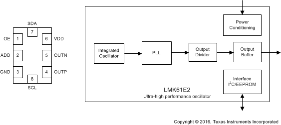
LMK61E2 pinout_functional_block_diagram_snas674.gif

4 修订历史记录

Changes from A Revision (September 2015) to B Revision

  • 添加了用于定制设计的 WEBENCH 链接和信息Go
  • 发布了新的 LMK61E2BAA、LMK61E2BBAGo
  • 将数据表文本更新为最新的文档和转换标准 Go
  • Moved Figure 34 to Layout ExampleGo

Changes from * Revision (September 2015) to A Revision

  • Moved conditions from figure title to table under each graphicGo
  • Updated Figure 26 Go
  • 添加了“相关文档”部分。Go

5 Pin Configuration and Functions

SIA Package
8-Pin QFM
Top View
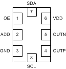
LMK61E2 pinout_snas674.gif

Pin Functions

PIN I/O DESCRIPTION
NAME NO.
POWER
GND 3 Ground Device Ground.
VDD 6 Analog 3.3-V Power Supply.
OUTPUT BLOCK
OUTP, OUTN 4, 5 Universal Differential Output Pair (LVPECL, LVDS or HCSL).
DIGITAL CONTROL / INTERFACES
ADD 2 LVCMOS When left open, LSB of I2C slave address is set to 01. When tied to VDD, LSB of I2C slave address is set to 10. When tied to GND, LSB of I2C slave address is set to 00.
OE 1 LVCMOS Output Enable (internal pullup). When set to low, output pair is disabled and set at high impedance.
SCL 8 LVCMOS I2C Serial Clock (open-drain). Requires an external pullup resistor to VDD.
SDA 7 LVCMOS I2C Serial Data (bidirectional, open-drain). Requires an external pullup resistor to VDD.

6 Specifications

6.1 Absolute Maximum Ratings

over operating free-air temperature range (unless otherwise noted)(1)
MIN MAX UNIT
VDD Device supply voltage –0.3 3.6 V
VIN Output voltage for logic inputs –0.3 VDD + 0.3 V
VOUT Output voltage for clock outputs –0.3 VDD + 0.3 V
TJ Junction temperature 150 °C
Tstg Storage temperature –40 125 °C
(1) Stresses beyond those listed under Absolute Maximum Ratings may cause permanent damage to the device. These are stress ratings only, which do not imply functional operation of the device at these or any other conditions beyond those indicated under Recommended Operating Conditions. Exposure to absolute maximum-rated conditions for extended periods may affect device reliability.

6.2 ESD Ratings

VALUE UNIT
V(ESD) Electrostatic discharge Human-body model (HBM), per ANSI/ESDA/JEDEC JS-001(1) ±2000 V
Charged-device model (CDM), per JEDEC specification JESD22-C101(2) ±500
(1) JEDEC document JEP155 states that 500 V HBM allows safe manufacturing with a standard ESD control process.
(2) JEDEC document JEP157 states that 250 V CDM allows safe manufacturing with a standard ESD control process.

6.3 Recommended Operating Conditions

over operating free-air temperature range (unless otherwise noted)
MIN NOM MAX UNIT
VDD Device supply voltage 3.135 3.3 3.465 V
TA Ambient temperature –40 25 85 °C
TJ Junction temperature 125 °C
tRAMP VDD power-up ramp time 0.1 100 ms

6.4 Thermal Information

THERMAL METRIC(1) LMK61E2 (2) (3) (4) UNIT
QFM (SIA)
8 PINS
AIRFLOW (LFM) 0 AIRFLOW (LFM) 200 AIRFLOW (LFM) 400
RθJA Junction-to-ambient thermal resistance 54 44 41.2 °C/W
RθJC(top) Junction-to-case (top) thermal resistance 34 n/a n/a °C/W
RθJB Junction-to-board thermal resistance 36.7 n/a n/a °C/W
ψJT Junction-to-top characterization parameter 11.2 16.9 21.9 °C/W
ψJB Junction-to-board characterization parameter 36.7 37.8 38.9 °C/W
RθJC(bot) Junction-to-case (bottom) thermal resistance n/a n/a n/a °C/W
(1) For more information about traditional and new thermal metrics, see the Semiconductor and IC Package Thermal Metrics application report.
(2) The package thermal resistance is calculated on a 4-layer JEDEC board.
(3) Connected to GND with 3 thermal vias (0.3-mm diameter).
(4) ψJB (junction-to-board) is used when the main heat flow is from the junction to the GND pad. See the Layout section for more information on ensuring good system reliability and quality.

6.5 Electrical Characteristics - Power Supply(1)

VDD = 3.3 V ± 5%, TA = –40°C to 85°C
PARAMETER TEST CONDITIONS MIN TYP MAX UNIT
IDD Device current consumption LVPECL(2) 162 208 mA
LVDS 152 196
HCSL 155 196
IDD-PD Device current consumption when output is disabled OE = GND 136 mA
(1) See Parameter Measurement Information for relevant test conditions.
(2) On-chip power dissipation should exclude 40 mW, dissipated in the 150-Ω termination resistors, from total power dissipation.

6.6 LVPECL Output Characteristics(1)

VDD = 3.3 V ± 5%, TA = –40°C to 85°C
PARAMETER TEST CONDITIONS MIN TYP MAX UNIT
fOUT Output frequency(2) 10 1000 MHz
VOD Output voltage swing
(VOH – VOL)(2)
700 800 1200 mV
VOUT, DIFF, PP Differential output peak-to-peak swing 2 × |VOD| V
VOS Output common-mode voltage VDD – 1.55 V
tR / tF Output rise/fall time (20% to 80%)(3) 120 200 ps
PN-Floor Output phase noise floor (fOFFSET > 10 MHz) 156.25 MHz –165 dBc/Hz
ODC Output duty cycle(3) 45% 55%
(1) See Parameter Measurement Information for relevant test conditions.
(2) An output frequency over fOUT max spec is possible, but output swing may be less than VOD min spec.
(3) Ensured by characterization.

6.7 LVDS Output Characteristics(1)

VDD = 3.3 V ± 5%, TA = –40°C to 85°C
PARAMETER TEST CONDITIONS MIN TYP MAX UNIT
fOUT Output frequency(1) 10 900 MHz
VOD Output voltage swing
(VOH – VOL)(1)
300 390 480 mV
VOUT, DIFF, PP Differential output peak-to-peak swing 2 × |VOD| V
VOS Output common-mode voltage 1.2 V
tR / tF Output rise/fall time (20% to 80%)(2) 150 250 ps
PN-Floor Output phase noise floor (fOFFSET > 10 MHz) 156.25 MHz –162 dBc/Hz
ODC Output duty cycle(2) 45% 55%
ROUT Differential output impedance 125 Ω
(1) An output frequency over fOUT max spec is possible, but output swing may be less than VOD min spec.
(2) Ensured by characterization.

6.8 HCSL Output Characteristics(1)

VDD = 3.3 V ± 5%, TA = –40°C to 85°C
PARAMETER TEST CONDITIONS MIN TYP MAX UNIT
fOUT Output frequency 10 400 MHz
VOH Output high voltage 600 850 mV
VOL Output low voltage –100 100 mV
VCROSS Absolute crossing voltage(2)(3) 250 475 mV
VCROSS-DELTA Variation of VCROSS(2)(3) 0 140 mV
dV/dt Slew rate(4) 0.8 2 V/ns
PN-Floor Output phase noise floor (fOFFSET > 10 MHz) 100 MHz –164 dBc/Hz
ODC Output duty cycle(4) 45% 55%
(1) See Parameter Measurement Information for relevant test conditions.
(2) Measured from –150 mV to +150 mV on the differential waveform with the 300-mVpp measurement window centered on the differential zero crossing.
(3) Ensured by design.
(4) Ensured by characterization.

6.9 OE Input Characteristics

VDD = 3.3 V ± 5%, TA = –40°C to 85°C
PARAMETER TEST CONDITIONS MIN TYP MAX UNIT
VIH Input high voltage 1.4 V
VIL Input low voltage 0.6 V
IIH Input high current VIH = VDD –40 40 µA
IIL Input low current VIL = GND –40 40 µA
CIN Input capacitance 2 pF

6.10 ADD Input Characteristics

VDD = 3.3 V ± 5%, TA = –40°C to 85°C
PARAMETER TEST CONDITIONS MIN TYP MAX UNIT
VIH Input high voltage 1.4 V
VIL Input low voltage 0.4 V
IIH Input high current VIH = VDD –40 40 µA
IIL Input low current VIL = GND –40 40 µA
CIN Input capacitance 2 pF

6.11 Frequency Tolerance Characteristics(1)

VDD = 3.3 V ± 5%, TA = –40°C to 85°C
PARAMETER TEST CONDITIONS MIN TYP MAX UNIT
fT Total frequency tolerance All output formats, frequency bands and device junction temperature up to 125°C; includes initial freq tolerance, temperature & supply voltage variation, solder reflow and aging (10 years) –50 50 ppm
(1) Ensured by characterization.

6.12 Power-On/Reset Characteristics (VDD)

VDD = 3.3 V ± 5%, TA = –40°C to 85°C
PARAMETER TEST CONDITIONS MIN TYP MAX UNIT
VTHRESH Threshold voltage(1) 2.72 2.95 V
VDROOP Allowable voltage droop(2) 0.1 V
tSTARTUP Start-up time (1) Time elapsed from VDD at 3.135 V to output enabled 10 ms
tOE-EN Output enable time(2) Time elapsed from OE at VIH to output enabled 50 µs
tOE-DIS Output disable time(2) Time elapsed from OE at VIL to output disabled 50 µs
(1) Ensured by characterization.
(2) Ensured by design.

6.13 I2C-Compatible Interface Characteristics (SDA, SCL)(1)(2)

VDD = 3.3 V ± 5%, TA = –40°C to 85°C
PARAMETER TEST CONDITIONS MIN TYP MAX UNIT
VIH Input high voltage 1.2 V
VIL Input low voltage 0.6 V
IIH Input leakage –40 40 µA
CIN Input capacitance 2 pF
COUT Input capacitance 400 pF
VOL Output low voltage IOL = 3 mA 0.6 V
fSCL I2C clock rate 100 400 kHz
tSU_STA START condition setup time SCL high before SDA low 0.6 µs
tH_STA START condition hold time SCL low after SDA low 0.6 µs
tPH_SCL SCL pulse width high 0.6 µs
tPL_SCL SCL pulse width low 1.3 µs
tH_SDA SDA hold time SDA valid after SCL low 0 0.9 µs
tSU_SDA SDA setup time 115 ns
tR_IN / tF_IN SCL/SDA input rise and fall time 300 ns
tF_OUT SDA output fall time CBUS = 10 pF to 400 pF 250 ns
tSU_STOP STOP condition setup time 0.6 µs
tBUS Bus free time between STOP and START 1.3 µs
(1) Total capacitive load for each bus line ≤ 400 pF.
(2) Ensured by design.

6.14 PSRR Characteristics(1)

VDD = 3.3 V, TA = 25°C, PLL bandwidth = 400 kHz, VCO Frequency = 5 GHz (Integer-N PLL), Output Divider = 32, Output Type = LVPECL/LVDS/HCSL
PARAMETER TEST CONDITIONS MIN TYP MAX UNIT
PSRR Spurs induced by 50-mV power supply ripple(2)(3) at 156.25-MHz output, all output types Sine wave at 50 kHz –70 dBc
Sine wave at 100 kHz –70
Sine wave at 500 kHz –70
Sine wave at 1 MHz –70
(1) See Parameter Measurement Information for relevant test conditions.
(2) Measured maximum spur level with 50-mVpp sinusoidal signal between 50 kHz and 1 MHz applied on VDD pin
(3) DJSPUR (ps, pk-pk) = [2 × 10(SPUR/20) / (π × fOUT)] × 1e6, where PSRR or SPUR in dBc and fOUT in MHz.

6.15 Other Characteristics

VDD = 3.3 V ± 5%, TA = –40°C to 85°C
PARAMETER TEST CONDITIONS MIN TYP MAX UNIT
fVCO VCO frequency range 4.6 5.6 GHz

6.16 PLL Clock Output Jitter Characteristics(1)(3)

VDD = 3.3 V ± 5%, TA = –40°C to 85°C
PARAMETER TEST CONDITIONS MIN TYP MAX UNIT
RJ RMS phase jitter(2)
(12 kHz – 20 MHz)
(1 kHz – 5 MHz)
fOUT ≥ 100 MHz, Integer-N PLL, All output types 100 200 fs RMS
RJ RMS phase jitter(2)
(12 kHz – 20 MHz)
(1 kHz – 5 MHz)
fOUT ≥ 100 MHz, Fractional-N PLL, All output types 150 300 fs RMS
(1) See Parameter Measurement Information for relevant test conditions.
(2) Ensured by characterization.
(3) Phase jitter measured with Agilent E5052 signal source analyzer using a differential-to-single ended converter (balun or buffer).

6.17 Typical 156.25-MHz Output Phase Noise Characteristics(1)(2)

VDD = 3.3 V, TA = 25°C, PLL bandwidth = 400 kHz, VCO Frequency = 5 GHz, Integer-N PLL, Output Divider = 32, Output Type = LVPECL/LVDS/HCSL
PARAMETER OUTPUT TYPE UNIT
LVPECL LVDS HCSL
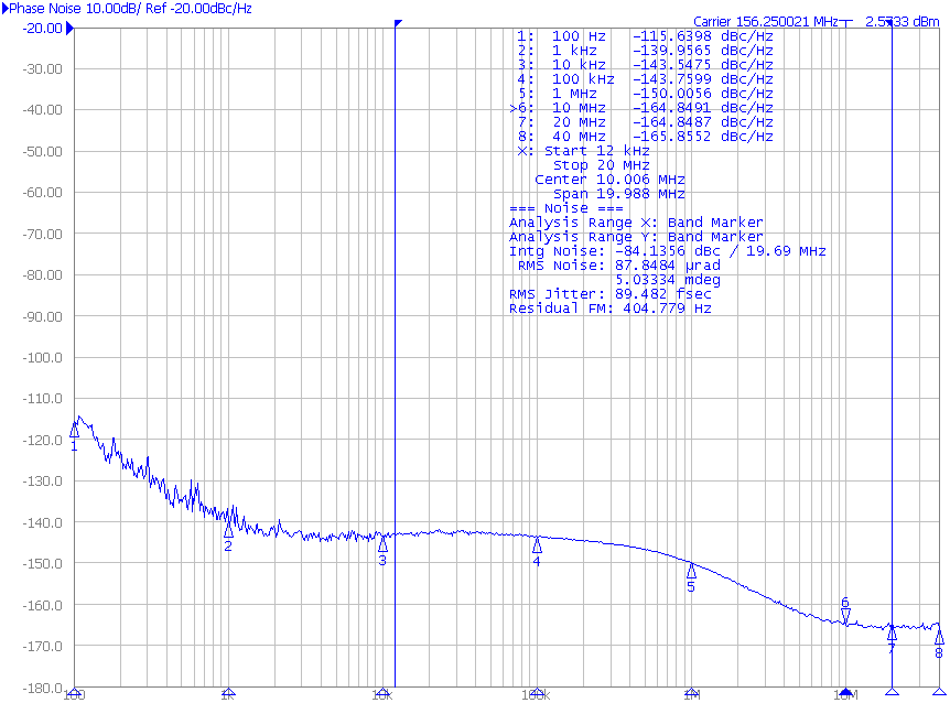
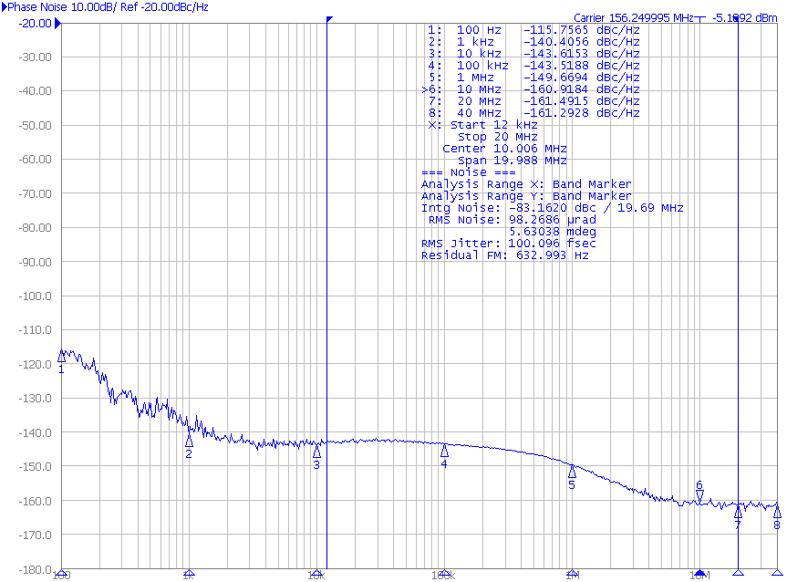
phn10k Phase noise at 10-kHz offset –143 –143 –143 dBc/Hz
Phn20k Phase noise at 20-kHz offset –143 –143 –143 dBc/Hz
phn100k Phase noise at 100-kHz offset –144 –144 –144 dBc/Hz
Phn200k Phase noise at 200-kHz offset –145 –145 –145 dBc/Hz
phn1M Phase noise at 1-MHz offset –150 –150 –150 dBc/Hz
phn2M Phase noise at 2-MHz offset –154 –154 –154 dBc/Hz
phn10M Phase noise at 10-MHz offset –165 –162 –164 dBc/Hz
phn20M Phase noise at 20-MHz offset –165 –162 –164 dBc/Hz
(1) See Parameter Measurement Information for relevant test conditions.
(2) Phase jitter measured with Agilent E5052 signal source analyzer using a differential-to-single ended converter (balun or buffer).

6.18 Typical 161.1328125 MHz Output Phase Noise Characteristics(1)(2)

VDD = 3.3 V, TA = 25°C, PLL bandwidth = 400 kHz, VCO Frequency = 5.15625 GHz, Fractional-N PLL, Output Divider = 32, Output Type = LVPECL/LVDS/HCSL
PARAMETER OUTPUT TYPE UNIT
LVPECL LVDS HCSL
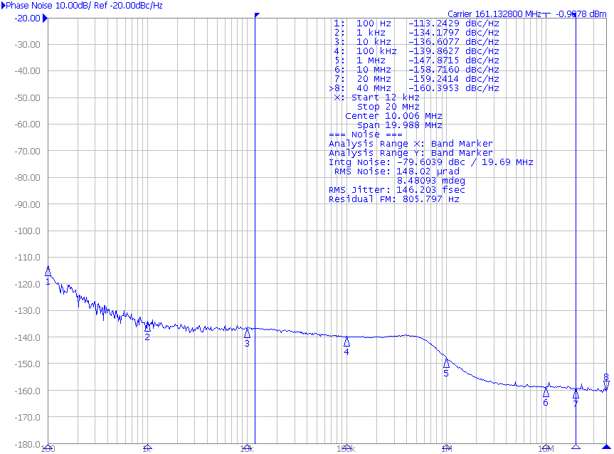
phn10k Phase noise at 10-kHz offset –136 –136 –136 dBc/Hz
phn20k Phase noise at 20-kHz offset –136 –136 –136 dBc/Hz
phn100k Phase noise at 100-kHz offset –140 –140 –140 dBc/Hz
phn200k Phase noise at 200-kHz offset –141 –141 –141 dBc/Hz
phn1M Phase noise at 1-MHz offset –148 –148 –148 dBc/Hz
phn2M Phase noise at 2-MHz offset –156 –156 –156 dBc/Hz
phn10M Phase noise at 10-MHz offset –161 –159 –160 dBc/Hz
phn20M Phase noise at 20-MHz offset –162 –160 –161 dBc/Hz
(1) See Parameter Measurement Information for relevant test conditions.
(2) Phase jitter measured with Agilent E5052 signal source analyzer using a differential-to-single ended converter (balun or buffer).

6.19 Additional Reliability and Qualification

PARAMETER CONDITION / TEST METHOD
Mechanical Shock MIL-STD-202, Method 213
Mechanical Vibration MIL-STD-202, Method 204
Moisture Sensitivity Level J-STD-020, MSL3

6.20 Typical Characteristics

LMK61E2 D001_SNAS674.png
PLL Bandwidth = 400 kHz VCO Frequency = 5 GHz
Integer-N PLL Output Divider = 32
Figure 1. Closed-Loop Phase Noise of LVPECL Differential Output at 156.25 MHz
LMK61E2 D003_SNAS674.png
PLL Bandwidth = 400 kHz VCO Frequency = 5 GHz
Integer-N PLL Output Divider = 32
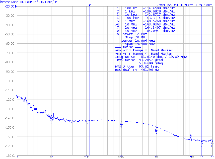
Figure 3. Closed-Loop Phase Noise of HCSL Differential Output at 156.25 MHz
LMK61E2 D005_SNAS674.png
PLL Bandwidth = 400 kHz VCO Frequency = 5.15625 GHz
Fractional-N PLL Output Divider = 32
Figure 5. Closed-Loop Phase Noise of LVDS Differential Output at 161.1328125 MHz
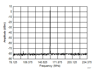
LMK61E2 D007_SNAS674.gif
PLL Bandwidth = 400 kHz VCO Frequency = 5 GHz
Integer-N PLL Output Divider = 32
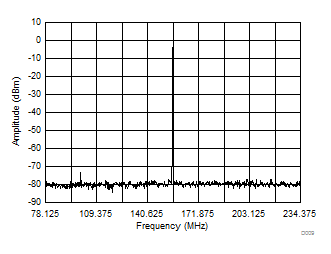
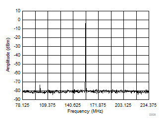
Figure 7. 156.25 ± 78.125-MHz LVPECL Differential Output Spectrum
LMK61E2 D009_SNAS674.gif
PLL Bandwidth = 400 kHz VCO Frequency = 5 GHz
Integer-N PLL Output Divider = 32
Figure 9. 156.25 ± 78.125-MHz HCSL Differential Output Spectrum
LMK61E2 D011_SNAS674.gif
PLL Bandwidth = 400 kHz VCO Frequency = 5.15625 GHz
Fractional-N PLL Output Divider = 32
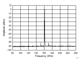
Figure 11. 161.1328125 ± 80.56640625-MHz LVDS Output Spectrum
LMK61E2 D013_SNAS674.gif
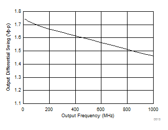
Figure 13. LVPECL Differential Output Swing vs Frequency
LMK61E2 D015_SNAS674.gif
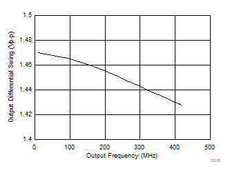
Figure 15. HCSL Differential Output Swing vs Frequency
LMK61E2 D002_SNAS674.png
PLL Bandwidth = 400 kHz VCO Frequency = 5 GHz
Integer-N PLL Output Divider = 32
Figure 2. Closed-Loop Phase Noise of LVDS Differential Output at 156.25 MHz
LMK61E2 D004_SNAS674.png
PLL Bandwidth = 400 kHz VCO Frequency = 5.15625 GHz
Fractional-N PLL Output Divider = 32
Figure 4. Closed-Loop Phase Noise of LVPECL Differential Output at 161.1328125 MHz
LMK61E2 D006_SNAS674.png
PLL Bandwidth = 400 kHz VCO Frequency = 5.15625 GHz
Fractional-N PLL Output Divider = 32
Figure 6. Closed-Loop Phase Noise of HCSL Differential Output at 161.1328125 MHz
LMK61E2 D008_SNAS674.gif
PLL Bandwidth = 400 kHz VCO Frequency = 5 GHz
Integer-N PLL Output Divider = 32
Figure 8. 156.25 ± 78.125-MHz LVDS Differential Output Spectrum
LMK61E2 D010_SNAS674.gif
PLL Bandwidth = 400 kHz VCO Frequency = 5.15625 GHz
Fractional-N PLL Output Divider = 32
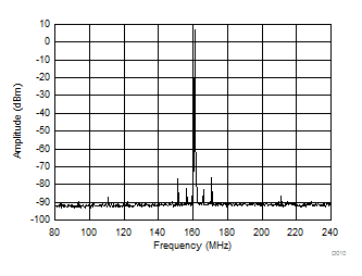
Figure 10. 161.1328125 ± 80.56640625-MHz LVPECL Differential Output Spectrum
LMK61E2 D012_SNAS674.gif
PLL Bandwidth = 400 kHz VCO Frequency = 5.15625 GHz
Fractional-N PLL Output Divider = 32
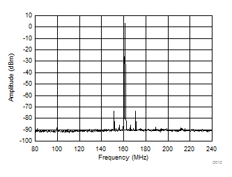
Figure 12. 161.1328125 ± 80.56640625-MHz HCSL Output Spectrum
LMK61E2 D014_SNAS674.gif
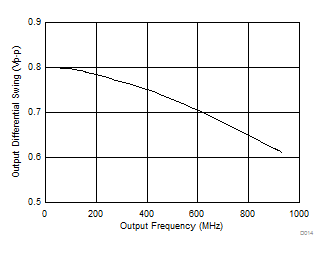
Figure 14. LVDS Differential Output Swing vs Frequency

7 Parameter Measurement Information

7.1 Device Output Configurations

LMK61E2 lvpecl_output_dc_configuration_snas674.gif Figure 16. LVPECL Output DC Configuration During Device Test
LMK61E2 lvds_output_dc_configuration_snas674.gif Figure 17. LVDS Output DC Configuration During Device Test
LMK61E2 hcsl_output_dc_configuration_snas674.gif Figure 18. HCSL Output DC Configuration During Device Test
LMK61E2 lvpecl_output_ac_configuration_snas677.gif Figure 19. LVPECL Output AC Configuration During Device Test
LMK61E2 lvds_output_ac_configuration_snas677.gif Figure 20. LVDS Output AC Configuration During Device Test
LMK61E2 hcsl_output_ac_configuration_snas677.gif Figure 21. HCSL Output AC Configuration During Device Test
LMK61E2 psrr_test_setup_snas674.gif Figure 22. PSRR Test Setup
LMK61E2 differential_output_voltage_rise_fall_time_snas674.gif Figure 23. Differential Output Voltage and Rise/Fall Time

8 Detailed Description

8.1 Overview

The LMK61E2 is a programmable oscillator that generates commonly used reference clocks with less than 200-fs RMS maximum random jitter in integer PLL mode and less than 300-fs RMS maximum random jitter in fractional PLL mode.

8.2 Functional Block Diagram

LMK61E2 new_block_diagram_snas674.gif

NOTE

Control blocks are compatible with 1.8, 2.5, or 3.3-V I/O voltage levels.

8.3 Feature Description

8.3.1 Device Block-Level Description

The LMK61E2 comprises of an integrated oscillator that includes a 50-MHz crystal, a fractional PLL with integrated VCO that supports a frequency range of 4.6 GHz to 5.6 GHz. The PLL block consists of a phase frequency detector (PFD), charge pump, integrated passive loop filter, a feedback divider that can support both integer and fractional values and a delta-sigma engine for noise suppression in fractional PLL mode. Completing the device is the combination of an integer output divider and a universal differential output buffer. The PLL is powered by on-chip low dropout (LDO) linear voltage regulators and the regulated supply network is partitioned such that the sensitive analog supplies are running from separate LDOs than the digital supplies which use their own LDO. The LDOs provide isolation to the PLL from any noise in the external power supply rail with a PSRR of better than –70 dBc at 50-kHz to 1-MHz ripple frequencies at 3.3-V device supply. The device supports fine and coarse frequency margining by changing the settings of the integrated oscillator and the output divider respectively.

8.3.2 Device Configuration Control

The LMK61E2 supports I2C programming interface where an I2C host can update any device configuration after the device enables the host interface and the host writes a sequence that updates the device registers. Once the device configuration is set, the host can also write to the on-chip EEPROM for a new set of power-up defaults based on the configuration pin settings in the soft pin configuration mode.

8.3.3 Register File Reference Convention

Figure 24 shows the method that this document employs to refer to an individual register bit or a grouping of register bits. If a drawing or text references an individual bit the format is to specify the register number first and the bit number second. The LMK61E2 contains 38 registers that are 8 bits wide. The register addresses and the bit positions both begin with the number zero (0). A period separates the register address and bit address. The first bit in the register file is address ‘R0.0’ meaning that it is located in Register 0 and is bit position 0. The last bit in the register file is address ‘R72.7’ referring to the 8th bit of register address 72 (the 73rd register in the device). Figure 24 also lists specific bit positions as a number contained within a box. A box with the register address encloses the group of boxes that represent the bits relevant to the specific device circuitry in context.

LMK61E2 lmk61e2_register_reference_format_snas674.gif Figure 24. LMK61E2 Register Reference Format

8.3.4 Configuring the PLL

The PLL in LMK61E2 can be configured to accommodate various output frequencies either through I2C programming interface or in the absence of programming, the PLL defaults stored in EEPROM is loaded on power up. The PLL can be configured by setting the Reference Doubler, Integrated PLL Loop Filter, Feedback Divider, and Output Divider.

For the PLL to operate in closed-loop mode, the following condition in Equation 1 has to be met.

Equation 1. FVCO = FREF × D × [(INT + NUM/DEN)]

where

  • FVCO: PLL/VCO Frequency (4.6 GHz to 5.6 GHz)
  • FREF: 50-MHz reference input
  • D: PLL input frequency doubler, 1=Disabled, 2=Enabled
  • INT: PLL feedback divider integer value (12 bits, 1 to 4095)
  • NUM: PLL feedback divider fractional numerator value (22 bits, 0 to 4194303)
  • DEN: PLL feedback divider fractional denominator value (22 bits, 1 to 4194303)

The output frequency is related to the VCO frequency as given in Equation 2.

Equation 2. FOUT = FVCO / OUTDIV

where

  • OUTDIV: Output divider value (9 bits, 5 to 511)

8.3.5 Integrated Oscillator

The integrated oscillator in LMK61E2 features programmable load capacitances that can be set to either operate at exactly its nominal oscillation frequency or operate at a fixed frequency offset from its nominal oscillation frequency. This is done by programming R16 and R17. More details on frequency margining are provided in Fine Frequency Margining.

8.3.6 Reference Doubler

The reference path has a frequency doubler that can be enabled by programming R34.5 = 1. Enabling the doubler allows a higher comparison frequency for the PLL and would result in a 3-dB reduction in the in-band phase noise at the output of the LMK61E2. Enabling the doubler also results in higher reference and phase detector spurs which will be minimized by enabling the higher order components (R3, C3) of the loop filter and programmed to appropriate values. Disabling the doubler would result in higher in-band phase noise on the device output than when the doubler is enabled but the reference and phase detector spurs would be lower on the device output than when the doubler is enabled.

8.3.7 Phase Frequency Detector

The Phase Frequency Detector (PFD) of the PLL takes inputs from the reference path and the feedback divider output and produces an output that is dependent on the phase and frequency difference between the two inputs. The input frequency of the PFD is 50 MHz when reference doubler is disabled, or 100 MHz when reference doubler is enabled.

8.3.8 Feedback Divider (N)

The N divider of the PLL includes fractional compensation and can achieve any fractional denominator (DEN) from 1 to 4,194,303. The integer portion, INT, is the whole part of the N divider value and the fractional portion, NUM / DEN, is the remaining fraction. INT, NUM, and DEN are programmed in R25, R26, R27, R28, R29, R30, R31, and R32. The total programmed N divider value, N, is determined by: N = INT + NUM / DEN. The output of the N divider sets the PFD frequency to the PLL and should equal 50 MHz, when reference doubler is disabled, or 100 MHz, when reference doubler is enabled.

8.3.9 Fractional Circuitry

The delta signal modulator is a key component of the fractional circuitry and is involved in noise shaping for better phase noise and spurs in the band of interest. The order of the delta sigma modulator is selectable between integer mode and third order, for fractional PLL mode, and can be programmed in R33[1-0]. Dithering can be programmed in R33[3-2] and should be disabled for integer PLL mode and set to weak for fractional PLL mode.

8.3.10 Charge Pump

The PLL has charge pump slices of 1.6 mA, to be used when PLL is set to fractional mode, or 6.4 mA, to be used when PLL is set to integer mode. These slices can be selected by programming R34[3-0]. When PLL is set to fractional mode, a phase shift needs to be introduced to maintain a linear response and ensure consistent performance across operating conditions and a value of 0x2 should be programmed in R35[6-4]. When PLL is set to integer mode, a value of 0x0 should be programmed in R35[6-4].

8.3.11 Loop Filter

The LMK61E2 features a fully integrated loop filter for the PLL and supports programmable loop bandwidth from 100 kHz to 1 MHz. The loop filter components, R2, C1, R3, and C3 can be configured by programming R36, R37, R38, and R39 respectively. The LMK61E2 features a fixed value of C2 of 10 nF. When PLL is configured in the fractional mode, R35.2 should be set to 1. When reference doubler is disabled for integer mode PLL, R35.2 should be set to 0 and R38[6-0] should be set to 0x00. When reference doubler is enabled for integer mode PLL, R35.2 should be set to 1 and R38 and R39 are written with the appropriate values. Figure 25 shows the loop filter structure of the PLL. It is important to set the PLL to best possible bandwidth to minimize output jitter. TI provides the WEBENCH® Clock Architect Tool that makes it easy to select the right loop filter components.

LMK61E2 loop_filter_structure_pll_snas674.gif Figure 25. Loop Filter Structure of PLL

8.3.12 VCO Calibration

The PLL in LMK61E2 is made of LC VCO that is designed using high-Q monolithic inductors to oscillate between 4.6 GHz and 5.6 GHz and has low-phase noise characteristics. The VCO must be calibrated to ensure that the clock outputs deliver optimal phase noise performance. Fundamentally, a VCO calibration establishes an optimal operating point within the tuning range of the VCO. Setting R72.1 to 1 causes a VCO recalibration and is necessary after device reconfiguration. VCO calibration automatically occurs on device power up.

8.3.13 High-Speed Output Divider

The high-speed output divider supports divide values of 5 to 511 and are programmed in R22 and R23. The output divider also supports coarse frequency margining that can initiate as low as a 5% change in the output frequency.

8.3.14 High-Speed Clock Output

The clock output can be configured as LVPECL, LVDS, or HCSL by programming R21[1-0]. Interfacing to LVPECL, LVDS, or HCSL receivers are done either with direct coupling or with AC-coupling capacitor as shown in Figure 16 – Figure 21.

The LVDS output structure has integrated 125-Ω termination between each side (P and N) of the differential pair. The HCSL output structure is open drain and can be DC or AC coupled to HCSL receivers with appropriate termination scheme. The LVPECL output structure is an emitter follower requiring external termination.

8.3.15 Device Status

The PLL loss of lock and PLL calibration status can be monitored by reading R66[1-0]. These bits represent a logic-high interrupt output and are self-cleared once the readback is complete.

8.3.15.1 Loss of Lock

The PLL loss of lock detection circuit is a digital circuit that detects any frequency error, even a single cycle slip. Loss of lock may occur when an incorrect PLL configuration is programmed or the VCO has not been recalibrated.

8.4 Device Functional Modes

8.4.1 Interface and Control

The host (DSP, Microcontroller, FPGA, and so forth) configures and monitors the LMK61E2 through the I2C port. The host reads and writes to a collection of control and status bits called the register map. The device blocks can be controlled and monitored through a specific grouping of bits located within the register file. The host controls and monitors certain device Wide critical parameters directly through register control and status bits. In the absence of the host, the LMK61E2 can be configured to operate from its on-chip EEPROM. The EEPROM array is automatically copied to the device registers upon power up. The user has the flexibility to rewrite the contents of EEPROM from the SRAM up to a 100 times.

Within the device registers, there are certain bits that have read or write access. Other bits are read-only (an attempt to write to a read-only bit does not change the state of the bit). Certain device registers and bits are reserved, meaning that they must not be changed from their default reset state. Figure 26 shows interface and control blocks within LMK61E2 and the arrows refer to read access from and write access to the different embedded memories (EEPROM, SRAM).

LMK61E2 lmk61e2_interface_and_control_block_snas674.gif Figure 26. LMK61E2 Interface and Control Block

8.5 Programming

8.5.1 I2C Serial Interface

The I2C port on the LMK61E2 works as a slave device and supports both the 100-kHz standard mode and 400-kHz fast mode operations. Fast mode imposes a glitch tolerance requirement on the control signals. Therefore, the input receivers ignore pulses of less than 50 ns duration. The I2C timing is given in I2C-Compatible Interface Characteristics (SDA, SCL). The timing diagram is given in Figure 27.

LMK61E2 i2c_timing_diagram_snas674.gif Figure 27. I2C Timing Diagram

In an I2C bus system, the LMK61E2 acts as a slave device and is connected to the serial bus (data bus SDA and lock bus SCL). These are accessed via a 7-bit slave address transmitted as part of an I2C packet. Only the device with a matching slave address responds to subsequent I2C commands. In soft pin mode, the LMK61E2 allows up to three unique slave devices to occupy the I2C bus based on the pin strapping of ADD (tied to VDD, GND, or left open). The device slave address is 10110xx (the two LSBs are determined by the ADD pin).

During the data transfer through the I2C interface, one clock pulse is generated for each data bit transferred. The data on the SDA line must be stable during the high period of the clock. The high or low state of the data line can change only when the clock signal on the SCL line is low. The start data transfer condition is characterized by a high-to-low transition on the SDA line while SCL is high. The stop data transfer condition is characterized by a low-to-high transition on the SDA line while SCL is high. The start and stop conditions are always initiated by the master. Every byte on the SDA line must be eight bits long. Each byte must be followed by an acknowledge bit and bytes are sent MSB first. The I2C register structure of the LMK61E2 is shown in Figure 28.

LMK61E2 i2c_register_structure_snas674.gif Figure 28. I2C Register Structure

The acknowledge bit (A) or non-acknowledge bit (A’) is the 9th bit attached to any 8-bit data byte and is always generated by the receiver to inform the transmitter that the byte has been received (when A = 0) or not (when A’ = 0). A = 0 is done by pulling the SDA line low during the 9th clock pulse and A’ = 0 is done by leaving the SDA line high during the 9th clock pulse.

The I2C master initiates the data transfer by asserting a start condition which initiates a response from all slave devices connected to the serial bus. Based on the 8-bit address byte sent by the master over the SDA line (consisting of the 7-bit slave address (MSB first) and an R/W’ bit), the device whose address corresponds to the transmitted address responds by sending an acknowledge bit. All other devices on the bus remain idle while the selected device waits for data transfer with the master.

After the data transfer has occurred, stop conditions are established. In write mode, the master asserts a stop condition to end data transfer during the 10th clock pulse following the acknowledge bit for the last data byte from the slave. In read mode, the master receives the last data byte from the slave but does not pull SDA low during the 9th clock pulse. This is known as a non-acknowledge bit. By receiving the non-acknowledge bit, the slave knows the data transfer is finished and enters the idle mode. The master then takes the data line low during the low period before the 10th clock pulse, and high during the 10th clock pulse to assert a stop condition. A generic transaction is shown in Figure 29.

LMK61E2 generic_programming_sequence_snas674.gif Figure 29. Generic Programming Sequence

The LMK61E2 I2C interface supports Block Register Write/Read, Read/Write SRAM, and Read/Write EEPROM operations. For Block Register Write/Read operations, the I2C master can individually access addressed registers that are made of an 8-bit data byte. The offset of the indexed register is encoded in the register address, as described in Table 1.

Table 1. Slave Address Byte

DEVICE A6 A5 A4 A3 A2 ADD pin R/W
LMK61E2 1 0 1 1 0 0x0, 0x1 or 0x3 1/0

8.5.2 Block Register Write

The I2C Block Register Write transaction is illustrated in Figure 30 and consists of the following sequence.

  1. Master issues a Start Condition.
  2. Master writes the 7-bit Slave Address following by a Write bit.
  3. Master writes the 8-bit Register address as the CommandCode of the programming sequence.
  4. Master writes one or more data bytes each of which should be acknowledged by the slave. The slave increments the internal register address after each byte.
  5. Master issues a Stop Condition to terminate the transaction.
LMK61E2 block_register_write_programming_sequence_snas674.gif Figure 30. Block Register Write Programming Sequence

8.5.3 Block Register Read

The I2C Block Register Read transaction is illustrated in Figure 31 and consists of the following sequence.

  1. Master issues a Start Condition.
  2. Master writes the 7-bit Slave Address followed by a Write bit.
  3. Master writes the 8-bit Register address as the CommandCode of the programming sequence.
  4. Master issues a Repeated Start Condition.
  5. Master writes the 7-bit Slave Address following by a Read bit.
  6. Slave returns one or more data bytes as long as the Master continues to acknowledge them. The slave increments the internal register address after each byte.
  7. Master issues a Stop Condition to terminate the transaction.
LMK61E2 block_register_read_programming_sequence_snas674.gif Figure 31. Block Register Read Programming Sequence

8.5.4 Write SRAM

The on-chip SRAM is a volatile, shadow memory array used to temporarily store register data, and is intended only for programming the non-Volatile EEPROM. The SRAM has the identical data format as the EEPROM map. The register configuration data can be transferred to the SRAM array through special memory access registers in the register map. To successfully program the SRAM, the complete base array and at least one page should be written. The following details the programming sequence to transfer the device registers into the SRAM.

  1. Program the device registers to match a desired setting.
  2. Write a 1 to R49.6. This ensures that the device registers are copied to the SRAM.

The SRAM can also be written with particular values according to the following programming sequence.

  1. Write the SRAM address in R51.
  2. Write the desired data byte in R53 in the same I2C transaction and this data byte will be written to the address specified in the step above. Any additional access that is part of the same transaction will cause the SRAM address to be incremented and a write will take place to the next SRAM address. Access to SRAM will terminate at the end of current I2C transaction.

NOTE

It is possible to increment SRAM address incorrectly when 2 successive accesses are made to R51.

8.5.5 Write EEPROM

The on-chip EEPROM is a non-Volatile memory array used to permanently store register data for a custom device start-up configuration setting to initialize registers upon power up or POR. The EEPROM is comprised of bits shown in the EEPROM Map. The transfer must first happen to the SRAM and then to the EEPROM. During EEPROM write, R49.2 is a 1 and the EEPROM contents cannot be accessed. The following details the programming sequence to transfer the entire contents of SRAM to EEPROM.

  1. Make sure the Write SRAM procedure (Write SRAM) was done to commit the register settings to the SRAM with start-up configurations intended for programming to the EEPROM.
  2. Write 0xBE to R56. This provides basic protection from inadvertent programming of EEPROM.
  3. Write a 1 to R49.0. This programs the entire SRAM contents to EEPROM. Once completed, the contents in R48 will increment by 1. R48 contains the total number of EEPROM programming cycles that are successfully completed.
  4. Write 0x00 to R56 to protect against inadvertent programming of EEPROM.

8.5.6 Read SRAM

The contents of the SRAM can be read out, one word at a time, starting with that of the requested address. Following details the programming sequence for an SRAM read by address.

  1. Write the SRAM address in R51.
  2. The SRAM data located at the address specified in the step above can be obtained by reading R53 in the same I2C transaction. Any additional access that is part of the same transaction will cause the SRAM address to be incremented and a read will take place of the next SRAM address. Access to SRAM will terminate at the end of current I2C transaction.

NOTE

It is possible to increment SRAM address incorrectly when 2 successive accesses are made to R51.

8.5.7 Read EEPROM

The contents of the EEPROM can be read out, one word at a time, starting with that of the requested address. Following details the programming sequence for an EEPROM read by address.

  1. Write the EEPROM address in R51.
  2. The EEPROM data located at the address specified in the step above can be obtained by reading R52 in the same I2C transaction. Any additional access that is part of the same transaction will cause the EEPROM address to be incremented and a read will take place of the next EEPROM address. Access to EEPROM will terminate at the end of current I2C transaction.

NOTE

It is possible to increment EEPROM address incorrectly when 2 successive accesses are made to R51.

8.6 EEPROM Map

Any bit that is labeled as RESERVED should be written with a 0.

Byte # Bit7 Bit6 Bit5 Bit4 Bit3 Bit2 Bit1 Bit0
0 RESERVED RESERVED RESERVED RESERVED RESERVED RESERVED RESERVED RESERVED
1 RESERVED RESERVED RESERVED RESERVED RESERVED RESERVED RESERVED RESERVED
2 RESERVED RESERVED RESERVED RESERVED RESERVED RESERVED RESERVED RESERVED
3 RESERVED RESERVED RESERVED RESERVED RESERVED RESERVED RESERVED RESERVED
4 NVMSCRC[7] NVMSCRC[6] NVMSCRC[5] NVMSCRC[4] NVMSCRC[3] NVMSCRC[2] NVMSCRC[1] NVMSCRC[0]
5 NVMCNT[7] NVMCNT[6] NVMCNT[5] NVMCNT[4] NVMCNT[3] NVMCNT[2] NVMCNT[1] NVMCNT[0]
6 1 RESERVED RESERVED RESERVED RESERVED 1 RESERVED RESERVED
7 RESERVED RESERVED 1 RESERVED RESERVED RESERVED RESERVED 1
8 RESERVED RESERVED RESERVED RESERVED RESERVED RESERVED RESERVED RESERVED
9 SLAVEADR[7] SLAVEADR[6] SLAVEADR[5] SLAVEADR[4] SLAVEADR[3] RESERVED RESERVED RESERVED
10 EEREV[7] EEREV[6] EEREV[5] EEREV[4] EEREV[3] EEREV[2] EEREV[1] EEREV[0]
11 RESERVED PLL_PDN RESERVED RESERVED RESERVED RESERVED AUTOSTRT RESERVED
14 RESERVED RESERVED RESERVED RESERVED RESERVED 1 RESERVED 1
15 RESERVED XO_CAPCTRL[1] XO_CAPCTRL[0] XO_CAPCTRL[9] XO_CAPCTRL[8] XO_CAPCTRL[7] XO_CAPCTRL[6] XO_CAPCTRL[5]
16 XO_CAPCTRL[4] XO_CAPCTRL[3] XO_CAPCTRL[2] RESERVED RESERVED RESERVED RESERVED RESERVED
19 RESERVED RESERVED RESERVED RESERVED RESERVED RESERVED RESERVED OUT_SEL[2]
20 OUT_SEL[1] OUT_SEL[0] RESERVED RESERVED RESERVED RESERVED RESERVED RESERVED
21 RESERVED RESERVED RESERVED RESERVED RESERVED RESERVED RESERVED RESERVED
22 PLL_NDIV[11] PLL_NDIV[10] PLL_NDIV[9] PLL_NDIV[8] PLL_NDIV[7] PLL_NDIV[6] PLL_NDIV[5] PLL_NDIV[4]
23 PLL_NDIV[3] PLL_NDIV[2] PLL_NDIV[1] PLL_NDIV[0] PLL_NUM[21] PLL_NUM[20] PLL_NUM[19] PLL_NUM[18]
24 PLL_NUM[17] PLL_NUM[16] PLL_NUM[15] PLL_NUM[14] PLL_NUM[13] PLL_NUM[12] PLL_NUM[11] PLL_NUM[10]
25 PLL_NUM[9] PLL_NUM[8] PLL_NUM[7] PLL_NUM[6] PLL_NUM[5] PLL_NUM[4] PLL_NUM[3] PLL_NUM[2]
26 PLL_NUM[1] PLL_NUM[0] PLL_DEN[21] PLL_DEN[20] PLL_DEN[19] PLL_DEN[18] PLL_DEN[17] PLL_DEN[16]
27 PLL_DEN[15] PLL_DEN[14] PLL_DEN[13] PLL_DEN[12] PLL_DEN[11] PLL_DEN[10] PLL_DEN[9] PLL_DEN[8]
28 PLL_DEN[7] PLL_DEN[6] PLL_DEN[5] PLL_DEN[4] PLL_DEN[3] PLL_DEN[2] PLL_DEN[1] PLL_DEN[0]
29 PLL_
DTHRMODE[1]
PLL_DTHRMODE[0] PLL_ORDER[1] PLL_ORDER[0] RESERVED RESERVED PLL_D PLL_CP[3]
30 PLL_CP[2] PLL_CP[1] PLL_CP[0] PLL_CP_PHASE_
SHIFT[2]
PLL_CP_PHASE_
SHIFT[1]
PLL_CP_PHASE_
SHIFT[0]
PLL_ENABLE_
C3[2]
PLL_ENABLE_
C3[1]
31 PLL_ENABLE_
C3[0]
PLL_LF_R2[7] PLL_LF_R2[6] PLL_LF_R2[5] PLL_LF_R2[4] PLL_LF_R2[3] PLL_LF_R2[2] PLL_LF_R2[1]
32 PLL_LF_R2[0] PLL_LF_C1[2] PLL_LF_C1[1] PLL_LF_C1[0] PLL_LF_R3[6] PLL_LF_R3[5] PLL_LF_R3[4] PLL_LF_R3[3]
33 PLL_LF_R3[2] PLL_LF_R3[1] PLL_LF_R3[0] PLL_LF_C3[2] PLL_LF_C3[1] PLL_LF_C3[0] RESERVED RESERVED
34 RESERVED OUT_DIV[8] OUT_DIV[7] OUT_DIV[6] OUT_DIV[5] OUT_DIV[4] OUT_DIV[3] OUT_DIV[2]
35 OUT_DIV[1] OUT_DIV[0] RESERVED RESERVED RESERVED RESERVED RESERVED RESERVED

8.7 Register Map

The default/reset values for each register is specified for LMK61E2-I3.

Name Addr Reset Bit7 Bit6 Bit5 Bit4 Bit3 Bit2 Bit1 Bit0
VNDRID_BY1 0 0x10 VNDRID[15:8]
VNDRID_BY0 1 0x0B VNDRID[7:0]
PRODID 2 0x33 PRODID[7:0]
REVID 3 0x00 REVID[7:0]
SLAVEADR 8 0xB0 SLAVEADR[7:1] RESERVED
EEREV 9 0x00 EEREV[7:0]
DEV_CTL 10 0x01 RESERVED PLL_PDN RESERVED ENCAL AUTOSTRT
XO_CAPCTRL_
BY1
16 0x00 RESERVED XO_CAPCTRL[1:0]
XO_CAPCTRL_
BY0
17 0x00 XO_CAPCTRL[9:2]
DIFFCTL 21 0x01 DIFF_OUT_PD RESERVED OUT_SEL[1:0]
OUTDIV_BY1 22 0x00 RESERVED OUT_DIV[8]
OUTDIV_BY0 23 0x20 OUT_DIV[7:0]
PLL_NDIV_BY1 25 0x00 RESERVED PLL_NDIV[11:8]
PLL_NDIV_BY0 26 0x64 PLL_NDIV[7:0]
PLL_FRACNUM_
BY2
27 0x00 RESERVED PLL_NUM[21:16]
PLL_FRACNUM_
BY1
28 0x00 PLL_NUM[15:8]
PLL_FRACNUM_
BY0
29 0x00 PLL_NUM[7:0]
PLL_FRACDEN_
BY2
30 0x00 RESERVED PLL_DEN[21:16]
PLL_FRACDEN_
BY1
31 0x00 PLL_DEN[15:8]
PLL_FRACDEN_
BY0
32 0x00 PLL_DEN[7:0]
PLL_MASHCTRL 33 0x0C RESERVED PLL_DTHRMODE[1:0] PLL_ORDER[1:0]
PLL_CTRL0 34 0x24 RESERVED PLL_D RESERVED PLL_CP[3:0]
PLL_CTRL1 35 0x03 RESERVED PLL_CP_PHASE_SHIFT[2:0] RESERVED PLL_ENABLE_C3[2:0]
PLL_LF_R2 36 0x28 PLL_LF_R2[7:0]
PLL_LF_C1 37 0x00 RESERVED PLL_LF_C1[2:0]
PLL_LF_R3 38 0x00 RESERVED PLL_LF_R3[6:0]
PLL_LF_C3 39 0x00 RESERVED PLL_LF_C3[2:0]
PLL_CALCTRL 42 0x00 RESERVED PLL_CLSDWAIT[1:0] PLL_VCOWAIT[1:0]
NVMSCRC 47 0x00 NVMSCRC[7:0]
NVMCNT 48 0x00 NVMCNT[7:0]
NVMCTL 49 0x10 RESERVED REGCOMMIT NVMCRCERR NVMAUTOCRC NVMCOMMIT NVMBUSY NVMERASE NVMPROG
NVMLCRC 50 0x00 NVMLCRC[7:0]
MEMADR 51 0x00 RESERVED MEMADR[6:0]
NVMDAT 52 0x00 NVMDAT[7:0]
RAMDAT 53 0x00 RAMDAT[7:0]
NVMUNLK 56 0x00 NVMUNLK[7:0]
INT_LIVE 66 0x00 RESERVED LOL CAL
SWRST 72 0x00 RESERVED SWR2PLL RESERVED

8.7.1 Register Descriptions

8.7.1.1 VNDRID_BY1 Register; R0

VNDRID_BY1 and VNDRID_BY0 registers are used to store the unique 16-bit Vendor Identification number assigned to I2C vendors.

Bit # Field Type Reset EEPROM Description
[7:0] VNDRID[15:8] R 0x10 N Vendor Identification Number Byte 1.

8.7.1.2 VNDRID_BY0 Register; R1

VNDRID_BY1 and VNDRID_BY0 registers are used to store the unique 16-bit Vendor Identification number assigned to I2C vendors.

Bit # Field Type Reset EEPROM Description
[7:0] VNDRID[7:0] R 0x0B N Vendor Identification Number Byte 0.

8.7.1.3 PRODID Register; R2

The Product Identification Number is a unique 8-bit identification number used to identify the LMK61E2.

Bit # Field Type Reset EEPROM Description
[7:0] PRODID[7:0] R 0x33 N Product Identification Number.

8.7.1.4 REVID Register; R3

The REVID register is used to identify the LMK61E2 mask revision.

Bit # Field Type Reset EEPROM Description
[7:0] REVID[7:0] R 0x00 N Device Revision Number. The Device Revision Number is used to identify the LMK61E2 mask-set revision used to fabricate this device.

8.7.1.5 SLAVEADR Register; R8

The SLAVEADR register reflects the 7-bit I2C Slave Address value initialized from from on-chip EEPROM.

Bit # Field Type Reset EEPROM Description
[7:1] SLAVEADR[7:1] R 0x58 Y I2C Slave Address. This field holds the 7-bit Slave Address used to identify this device during I2C transactions. The two least significant bits of the address can be configured using ADD pin as shown.
SLAVEADR[2:1] ADD pin
0 (0x0) 0
1 (0x1) Float
3 (0x3) 1
[0] RESERVED - - N Reserved.

8.7.1.6 EEREV Register; R9

The EEREV register provides an EEPROM image revision record. EEPROM Image Revision is automatically retrieved from EEPROM and stored in the EEREV register after a reset or after a EEPROM commit operation.

Bit # Field Type Reset EEPROM Description
[7:0] EEREV[7:0] R 0x00 Y EEPROM Image Revision ID

8.7.1.7 DEV_CTL Register; R10

The DEV_CTL register holds the control functions described in the following table.

Bit # Field Type Reset EEPROM Description
[7] RESERVED - 0 Y Reserved.
[6] PLL_PDN RW 0 Y PLL Powerdown. The PLL_PDN bit determines whether PLL is automatically enabled and calibrated after a hardware reset. If the PLL_PDN bit is set to 1 during normal operation then PLL is disabled and the calibration circuit is reset. When PLL_PDN is then cleared to 0 PLL is re-enabled and the calibration sequence is automatically restarted.
PLL_PDN Value
0 PLL Enabled
1 PLL Disabled
[5:2] RESERVED[5:2] RW 0 Y Reserved.
[1] ENCAL RWSC 0 N Enable Frequency Calibration. Triggers PLL/VCO calibration on both PLLs in parallel on 0 –> 1 transition of ENCAL. This bit is self-clearing and set to a 0 after PLL/VCO calibration is complete. In powerup or software rest mode, AUTOSTRT takes precedence.
[0] AUTOSTRT RW 1 Y Autostart. If AUTOSTRT is set to 1 the device will automatically attempt to achieve lock and enable outputs after a device reset. A device reset can be triggered by the power-on-reset, RESETn pin or by writing to the RESETN_SW bit. If AUTOSTRT is 0 then the device will halt after the configuration phase, a subsequent write to set the AUTOSTRT bit to 1 will trigger the PLL Lock sequence.

8.7.1.8 XO_CAPCTRL_BY1 Register; R16

XO Margining Offset Value bits[9:8]

Bit # Field Type Reset EEPROM Description
[7:2] RESERVED[5:0] - - N Reserved.
[1:0] XO_CAPCTRL [1:0] RW 0x0 Y XO Offset Value bits [1:0]

8.7.1.9 XO_CAPCTRL_BY0 Register; R17

XO margining Offset Value bits[7:0]

Bit # Field Type Reset EEPROM Description
[7:0] XO_CAPCTRL [9:2] RW 0x80 Y XO Offset Value bits[9:2]

8.7.1.10 DIFFCTL Register; R21

The DIFFCTL register provides control over Output.

Bit # Field Type Reset EEPROM Description
[7] DIFF_OUT_PD RW 0 N Power down differential output buffer.
[6:2] RESERVED - - N Reserved.
[1:0] OUT_SEL[1:0] RW 0x1 Y Channel Output Driver Format Select. The OUT_SEL field controls the Channel Output Driver as shown below.
OUT_SEL OUTPUT OPERATION
0 (0x0) Tri-State
1 (0x1) LVPECL
2 (0x2) LVDS
3 (0x3) HCSL

8.7.1.11 OUTDIV_BY1 Register; R22

The 9-bit output integer divider value is set by the OUTDIV_BY1 and OUTDIV_BY0 registers.

Bit # Field Type Reset EEPROM Description
[7:1] RESERVED RW 0x00 Y Reserved.
[0] OUT_DIV[8] RW 0 Y Channel's Output Divider Byte 1 (Bit 8). The Channel Divider, OUT_DIV, is a 9-bit divider. The valid values for OUT_DIV range from 5 to 511 as shown below.
OUT_DIV DIVIDE RATIO
0-4 RESERVED
5 (0x005) 5
6 (0x006) 6
7 (0x007) 7
255 (0x0FF) 255
256 (0x100) 256
257 (0x101) 257
... ...
511 (0x1FF) 511

8.7.1.12 OUTDIV_BY0 Register; R23

The 9-bit output integer divider value is set by the OUTDIV_BY1 and OUTDIV_BY0 registers.

Bit # Field Type Reset EEPROM Description
[7:0] OUT_DIV[7:0] RW 0x20 Y Channel's Output Divider Byte 0 (Bits 7-0).

8.7.1.13 PLL_NDIV_BY1 Register; R25

The 12-bit N integer divider value for PLL is set by the PLL_NDIV_BY1 and PLL_NDIV_BY0 registers.

Bit # Field Type Reset EEPROM Description
[7:4] RESERVED - - N Reserved.
[3:0] PLL_NDIV[11:8] RW 0x0 Y PLL N Divider Byte 1. PLL Integer N Divider bits [11:8].

8.7.1.14 PLL_NDIV_BY0 Register; R26

The PLL_NDIV_BY0 register is described in the following table.

Bit # Field Type Reset EEPROM Description
[7:0] PLL_NDIV[7:0] RW 0x32 Y PLL N Divider Byte 0. PLL Integer N Divider bits [7:0].

8.7.1.15 PLL_FRACNUM_BY2 Register; R27

The 22-bit Fractional Divider Numerator value for PLL is set by registers PLL_FRACNUM_BY2, PLL_FRACNUM_BY1 and PLL_FRACNUM_BY0.

Bit # Field Type Reset EEPROM Description
[7:6] RESERVED - - N Reserved.
[5:0] PLL_NUM[21:16] RW 0x00 Y PLL Fractional Divider Numerator Byte 2. Bits [21:16]

8.7.1.16 PLL_FRACNUM_BY1 Register; R28

The PLL_FRACNUM_BY1 register is described in the following table.

Bit # Field Type Reset EEPROM Description
[7:0] PLL_NUM[15:8] RW 0x00 Y PLL Fractional Divider Numerator Byte 1. Bits [15:8].

8.7.1.17 PLL_FRACNUM_BY0 Register; R29

The PLL_FRACNUM_BY0 register is described in the following table.

Bit # Field Type Reset EEPROM Description
[7:0] PLL_NUM[7:0] RW 0x00 Y PLL Fractional Divider Numerator Byte 0. Bits [7:0].

8.7.1.18 PLL_FRACDEN_BY2 Register; R30

The 22-bit Fractional Divider Denominator value for PLL is set by registers PLL_FRACDEN_BY2, PLL_FRACDEN_BY1 and PLL_FRACDEN_BY0.

Bit # Field Type Reset EEPROM Description
[7:6] RESERVED - - N Reserved.
[5:0] PLL_DEN[21:16] RW 0x00 Y PLL Fractional Divider Denominator Byte 2. Bits [21:16].

8.7.1.19 PLL_FRACDEN_BY1 Register; R31

The PLL_FRACDEN_BY1 register is described in the following table.

Bit # Field Type Reset EEPROM Description
[7:0] PLL_DEN[15:8] RW 0x00 Y PLL Fractional Divider Denominator Byte 1. Bits [15:8].

8.7.1.20 PLL_FRACDEN_BY0 Register; R32

The PLL_FRACDEN_BY0 register is described in the following table.

Bit # Field Type Reset EEPROM Description
[7:0] PLL_DEN[7:0] RW 0x00 Y PLL Fractional Divider Denominator Byte 0. Bits [7:0].

8.7.1.21 PLL_MASHCTRL Register; R33

The PLL_MASHCTRL register provides control of the fractional divider for PLL.

Bit # Field Type Reset EEPROM Description
[7:4] RESERVED - - N Reserved.
[3:2] PLL_DTHRMODE[1:0] RW 0x3 Y Mash Engine dither mode control.
DITHERMODE Dither Configuration
0 (0x0) Weak
1 (0x1) Reserved
2 (0x2) Reserved
3 (0x3) Dither Disabled
[1:0] PLL_ORDER[1:0] RW 0x0 Y Mash Engine Order.
ORDER Order Configuration
0 (0x0) Integer Mode Divider
1 (0x1) Reserved
2 (0x2) Reserved
3 (0x3) 3rd order

8.7.1.22 PLL_CTRL0 Register; R34

The PLL_CTRL1 register provides control of PLL. The PLL_CTRL1 register fields are described in the following table.

Bit # Field Type Reset EEPROM Description
[7:6] RESERVED RW 0x0 Y Reserved.
[5] PLL_D RW 1 Y PLL R Divider Frequency Doubler Enable. If PLL_D is 1 the R Divider Frequency Doubler is enabled.
[4] RESERVED - - N Reserved.
[3:0] PLL_CP[3:0] RW 0x8 Y PLL Charge Pump Current. Other combinations of PLL_CP[3:0] not in table below are reserved and not supported.
PLL_CP[3:0] PLL Charge Pump Current
4 (0x4) 1.6 mA
8 (0x8) 6.4 mA

8.7.1.23 PLL_CTRL1 Register; R35

The PLL_CTRL3 register provides control of PLL. The PLL_CTRL3 register fields are described in the following table.

Bit # Field Type Reset EEPROM Description
[7] RESERVED - - N Reserved.
[6:4] PLL_CP_PHASE_SHIFT[2:0] RW 0x0 Y Program Charge Pump Phase Shift.
PLL_CP_PHASE_SHIFT[2:0] Phase Shift
0 (0x0) No delay
1 (0x1) 1.3 ns for 100 MHz fPD
2 (0x2) 1 ns for 100 MHz fPD
3 (0x3) 0.9 ns for 100 MHz fPD
4 (0x4) 1.3 ns for 50 MHz fPD
5 (0x5) 1 ns for 50 MHz fPD
6 (0x6) 0.9 ns for 50 MHz fPD
7 (0x7) 0.7 ns for 50 MHz fPD
[3] RESERVED - - N Reserved.
[2] PLL_ENABLE_C3 RW 0 Y Disable third order capacitor in the low pass filter.
PLL_ENABLE_C3 MODE
0 2nd order loop filter recommended setting
1 Enables C3, 3rd order loop filter enabled
[1:0] RESERVED - 0x3 Y Reserved.

8.7.1.24 PLL_LF_R2 Register; R36

The PLL_LF_R2 register controls the value of the PLL Loop Filter R2.

Bit # Field Type Reset EEPROM Description
[7:0] PLL_LF_R2[7:0] RW 0x08 Y PLL Loop Filter R2. NOTE: Table below lists commonly used R2 values but more selections are available.
PLL_LF_R2[7:0] R2 (Ω)
1 (0x01) 200
4 (0x04) 500
8 (0x08) 700
32 (0x20) 1600
48 (0x30) 2400
64 (0x40) 3200

8.7.1.25 PLL_LF_C1 Register; R37

The PLL_LF_C1 register controls the value of the PLL Loop Filter C1.

Bit # Field Type Reset EEPROM Description
[7:3] RESERVED - - N Reserved.
[2:0] PLL_LF_C1[2:0] RW 0x0 Y PLL Loop Filter C1. The value in pF is given by 5 + 50 * PLL_LF_C1 (in decimal).

8.7.1.26 PLL_LF_R3 Register; R38

The PLL_LF_R3 register controls the value of the PLL Loop Filter R3.

Bit # Field Type Reset EEPROM Description
[7] RESERVED - - N Reserved.
[6:0] PLL_LF_R3[6:0] RW 0x00 Y PLL Loop Filter R3. NOTE: Table below lists commonly used R3 values but more selections are available.
PLL_LF_R3[6:0] R3 (Ω)
0 (0x00) 18
3 (0x03) 205
8 (0x08) 854
9 (0x09) 1136
12 (0x0C) 1535
17 (0x11) 1936
20 (0x14) 2335

8.7.1.27 PLL_LF_C3 Register; R39

The PLL_LF_C3 register controls the value of the PLL Loop Filter C3.

Bit # Field Type Reset EEPROM Description
[7:3] RESERVED - - N Reserved.
[2:0] PLL_LF_C3[2:0] RW 0x0 Y PLL Loop Filter C3. The value in pF is given by 5 * PLL_LF_C3 (in decimal).

8.7.1.28 PLL_CALCTRL Register; R42

The PLL_CALCTRL register is described in the following table.

Bit # Field Type Reset EEPROM Description
[7:4] RESERVED - - N Reserved.
[3:2] PLL_CLSDWAIT[1:0] RW 0x2 Y Closed Loop Wait Period. The CLSDWAIT field sets the closed loop wait period. Recommended value is 0x2.
CLSDWAIT Anlog closed loop VCO stabilization time
0 (0x0) 150 µs
1 (0x1) 300 µs
2 (0x2) 500 µs
3 (0x3) 2000 µs
[1:0] PLL_VCOWAIT[1:0] RW 0x1 Y VCO Wait Period. Recommended value is 0x1.
VCOWAIT VCO stabilization time
0 (0x0) 20 µs
1 (0x1) 400 µs
2 (0x2) 4000 µs
3 (0x3) 10000 µs

8.7.1.29 NVMSCRC Register; R47

The NVMSCRC register holds the Stored CRC (Cyclic Redundancy Check) byte that has been retreived from on-chip EEPROM.

Bit # Field Type Reset EEPROM Description
[7:0] NVMSCRC[7:0] R 0x00 Y EEPROM Stored CRC.

8.7.1.30 NVMCNT Register; R48

The NVMCNT register is intended to reflect the number of on-chip EEPROM Erase/Program cycles that have taken place in EEPROM. The count is automatically incremented by hardware and stored in EEPROM.

Bit # Field Type Reset EEPROM Description
[7:0] NVMCNT[7:0] R 0x00 Y EEPROM Program Count. The NVMCNT increments automatically after every EEPROM Erase/Program Cycle. The NVMCNT value is retreived automatically after reset, after a EEPROM Commit operation or after a Erase/Program cycle. The NVMCNT register will increment until it reaches its maximum value of 255 after which no further increments will take place.

8.7.1.31 NVMCTL Register; R49

The NVMCTL register allows control of the on-chip EEPROM Memories.

Bit # Field Type Reset EEPROM Description
[7] RESERVED - - N Reserved.
[6] REGCOMMIT RWSC 0 N REG Commit to EEPROM SRAM Array. The REGCOMMIT bit is used to initiate a transfer from the on-chip registers back to the corresponding location in the EEPROM SRAM Array. The REGCOMMIT bit is automatically cleared to 0 when the transfer is complete.
[5] NVMCRCERR R 0 N EEPROM CRC Error Indication. The NVMCRCERR bit is set to 1 if a CRC Error has been detected when reading back from on-chip EEPROM during device configuration.
[4] NVMAUTOCRC RW 1 N EEPROM Automatic CRC. When NVMAUTOCRC is 1 then the EEPROM Stored CRC byte is automatically calculated whenever a EEPROM program takes place.
[3] NVMCOMMIT RWSC 0 N EEPROM Commit to Registers. The NVMCOMMIT bit is used to initiate a transfer of the on-chip EEPROM contents to internal registers. The transfer happens automatically after reset or when NVMCOMMIT is set to 1. The NVMCOMMIT bit is automatically cleared to 0. The I2C registers cannot be read while a EEPROM Commit operation is taking place.
[2] NVMBUSY R 0 N EEPROM Program Busy Indication. The NVMBUSY bit is 1 during an on-chip EEPROM Erase/Program cycle. While NVMBUSY is 1 the on-chip EEPROM cannot be accessed.
[1] NVMERASE RWSC 0 N EEPROM Erase Start. The NVMERASE bit is used to begin an on-chip EEPROM Erase cycle. The Erase cycle is only initiated if the immediately preceding I2C transaction was a write to the NVMUNLK register with the appropriate code. The NVMERASE bit is automatically cleared to 0. The EEPROM Erase operation takes around 115ms.
[0] NVMPROG RWSC 0 N EEPROM Program Start. The NVMPROG bit is used to begin an on-chip EEPROM Program cycle. The Program cycle is only initiated if the immediately preceding I2C transaction was a write to the NVMUNLK register with the appropriate code. The NVMPROG bit is automatically cleared to 0. If the NVMERASE and NVMPROG bits are set simultaneously then an ERASE/PROGRAM cycle will be executed The EEPROM Program operation takes around 115ms.

8.7.1.32 MEMADR Register; R51

The MEMADR register holds 7-bits of the starting address for on-chip SRAM or EEPROM access.

Bit # Field Type Reset EEPROM Description
[7] RESERVED - - N Reserved.
[6:0] MEMADR[6:0] RW 0x00 N Memory Address. The MEMADR value determines the starting address for on-chip SRAM read/write access or on-chip EEPROM access. The internal address to access SRAM or EEPROM is automatically incremented; however the MEMADR register does not reflect the internal address in this way. When the SRAM or EEPROM arrays are accessed using the I2C interface only bits [4:0] of MEMADR are used to form the byte Wise address.

8.7.1.33 NVMDAT Register; R52

The NVMDAT register returns the on-chip EEPROM contents from the starting address specified by the MEMADR register.

Bit # Field Type Reset EEPROM Description
[7:0] NVMDAT[7:0] R 0x00 N EEPROM Read Data. The first time an I2C read transaction accesses the NVMDAT register address, either because it was explicitly targeted or because the address was auto-incremented, the read transaction will return the EEPROM data located at the address specified by the MEMADR register. Any additional read's which are part of the same transaction will cause the EEPROM address to be incremented and the next EEPROM data byte will be returned. The I2C address will no longer be auto-incremented, i.e the I2C address will be locked to the NVMDAT register after the first access. Access to the NVMDAT register will terminate at the end of the current I2C transaction.

8.7.1.34 RAMDAT Register; R53

The RAMDAT register provides read and write access to the SRAM that forms part of the on-chip EEPROM module.

Bit # Field Type Reset EEPROM Description
[7:0] RAMDAT[7:0] RW 0x00 N RAM Read/Write Data. The first time an I2C read or write transaction accesses the RAMDAT register address, either because it was explicitly targeted or because the address was auto-incremented, a read transaction will return the RAM data located at the address specified by the MEMADR register and a write transaction will cause the current I2C data to be written to the address specified by the MEMADR register. Any additional accesses which are part of the same transaction will cause the RAM address to be incremented and a read or write access will take place to the next SRAM address. The I2C address will no longer be auto-incremented, i.e the I2C address will be locked to the RAMDAT register after the first access. Access to the RAMDAT register will terminate at the end of the current I2C transaction.

8.7.1.35 NVMUNLK Register; R56

The NVMUNLK register provides a rudimentary level of protection to prevent inadvertent programming of the on-chip EEPROM.

Bit # Field Type Reset EEPROM Description
[7:0] NVMUNLK[7:0] RW 0x00 N EEPROM Prog Unlock. The NVMUNLK register must be written immediately prior to setting the NVMPROG bit of register NVMCTL, otherwise the Erase/Program cycle will not be triggered. NVMUNLK must be written with a value of 0xBE.

8.7.1.36 INT_LIVE Register; R66

The INT_LIVE register reflects the current status of the interrupt sources.

Bit # Field Type Reset EEPROM Description
[7:2] RESERVED - - N Reserved.
[1] LOL R 0 N Loss of Lock PLL.
[0] CAL R 0 N Calibration Active PLL.

8.7.1.37 SWRST Register; R72

The SWRST1 register provides software reset control for specific on-chip modules. Each bit in this register is individually self cleared after a write operation. The SWRST1 register will always return 0x00 in a read transaction.

Bit # Field Type Reset EEPROM Description
[7:2] RESERVED - - N Reserved.
[1] SWR2PLL RWSC 0 N Software Reset PLL. Setting SWR2PLL to 1 resets the PLL calibrator and clock dividers. This bit is automatically cleared to 0.
[0] RESERVED - - N Reserved.

9 Application and Implementation

NOTE

Information in the following applications sections is not part of the TI component specification, and TI does not warrant its accuracy or completeness. TI’s customers are responsible for determining suitability of components for their purposes. Customers should validate and test their design implementation to confirm system functionality.

9.1 Application Information

The LMK61E2 is an ultra-low jitter programmable oscillator that can be used to provide reference clocks for high-speed serial links resulting in improved system performance. The LMK61E2 also supports a variety of features that aids the hardware designer during the system debug and validation phase.

9.2 Typical Applications

9.2.1 Jitter Considerations in Serdes Systems

Jitter-sensitive applications such as 10-Gbps or 100-Gbps Ethernet, deploy a serial link using a Serializer in the transmit section (TX) and a De-serializer in the receive section (RX). These SERDES blocks are typically embedded in an ASIC or FPGA. Estimating the clock jitter impact on the link budget requires understanding of the TX PLL bandwidth and the RX CDR bandwidth.

As can be seen in Figure 32, the pass band region between the TX low-pass cutoff and RX high-pass cutoff frequencies is the range over which the reference clock jitter adds without any attenuation to the jitter budget of the link. Outside of these frequencies, the SERDES link will attenuate the reference clock jitter with a 20 dB/dec or even steeper roll-off. Modern ASIC or FPGA designs have some flexibility on deciding the optimal RX CDR bandwidth and TX PLL bandwidth. These bandwidths are typically set based on what is achievable in the ASIC or FPGA process node, without increasing design complexity, and on any jitter tolerance or wander specification that needs to be met, as related to the RX CDR bandwidth.

The overall allowable jitter in a serial link is dictated by IEEE or other relevant standards. For example, IEEE802.3ba states that the maximum transmit jitter (peak-peak) for 10-Gbps Ethernet should be no more than 0.28 × UI and this equates to a 27.1516 ps, p-p for the overall allowable transmit jitter.

The jitter contributing elements are made up of the reference clock, generated potentially from a device like LMK61E2, the transmit medium, transmit driver, and so forth. Only a portion of the overall allowable transmit jitter is allocated to the reference clock, typically 20% or lower. Therefore, the allowable reference clock jitter, for a 20% clock jitter budget, is 5.43 ps, p-p.

Jitter in a reference clock is made up of deterministic jitter (arising from spurious signals due to supply noise or mixing from other outputs or from the reference input) and random jitter (usually due to thermal noise and other uncorrelated noise sources). A typical clock tree in a serial link system consists of clock generators and fanout buffers. The allowable reference clock jitter of 5.43 ps, p-p is needed at the output of the fanout buffer. Modern fanout buffers have low-additive random jitter (less than 100 fs RMS) with no substantial contribution to the deterministic jitter. Therefore, the clock generator and fanout buffer contribute to the random jitter while the primary contributor to the deterministic jitter is the clock generator. Rule of thumb, for modern clock generators, is to allocate 25% of allowable reference clock jitter to the deterministic jitter and 75% to the random jitter. This amounts to an allowable deterministic jitter of 1.36 ps, p-p and an allowable random jitter of 4.07 ps, p-p. For serial link systems that need to meet a bit error rate (BER) of 10–12, the allowable random jitter in root-mean-square is 0.29 ps RMS. This is calculated by dividing the p-p jitter by 14 for a BER of 10–12. Accounting for random jitter from the fanout buffer, the random jitter needed from the clock generator is 0.27 ps RMS. This is calculated by the root-mean-square subtraction from the desired jitter at the fanout buffer's output assuming 100 fs RMS of additive jitter from the fanout buffer.

With careful frequency planning techniques, like spur optimization (covered in Spur Mitigation Techniques ) and on-chip LDOs to suppress supply noise, the LMK61E2 is able to generate clock outputs with deterministic jitter that is below 1 ps, p-p and random jitter that is below 0.2 ps RMS. This gives the serial link system with additional margin on the allowable transmit jitter resulting in a BER better than 10–12.

LMK61E2 dependence_of_clock_jitter_serial_links_snas674.gif Figure 32. Dependence of Clock Jitter in Serial Links

9.2.2 Frequency Margining

9.2.2.1 Fine Frequency Margining

IEEE802.3 dictates that Ethernet frames stay compliant to the standard specifications when clocked with a reference clock that is within ±100 ppm of its nominal frequency. In the worst case, an RX node with its local reference clock at –100 ppm from its nominal frequency should be able to work seamlessly with a TX node that has its own local reference clock at +100 ppm from its nominal frequency. Without any clock compensation on the RX node, the read pointer will severely lag behind the write pointer and cause FIFO overflow errors. On the contrary, when the RX node’s local clock operates at +100 ppm from its nominal frequency and the TX node’s local clock operates at –100 ppm from its nominal frequency, FIFO underflow errors occur without any clock compensation.

To prevent such overflow and underflow errors from occurring, modern ASICs and FGPAs include a clock compensation scheme that introduces elastic buffers. Such a system, shown in Figure 33, is validated thoroughly during the validation phase by interfacing slower nodes with faster ones and ensuring compliance to IEEE802.3. The LMK61E2 provides the ability to fine tune the frequency of its outputs based on changing its load capacitance for the integrated oscillator. This fine tuning can be done through I2C as described in Integrated Oscillator. The change in load capacitance is implemented in a manner such that the output of LMK61E2 undergoes a smooth monotonic change in frequency.

9.2.2.2 Coarse Frequency Margining

Certain systems require the processors to be tested at clock frequencies that are slower or faster by 5% or 10%. The LMK61E2 offers the ability to change its output divider for the desired change from its nominal output frequency as explained in the High-Speed Output Divider section.

LMK61E2 system_implementation_clock_compensation_snas674.gif Figure 33. System Implementation With Clock Compensation for Standards Compliance

9.2.3 Design Requirements

Consider a typical wired communications application, like a top-of-rack switch, which needs to clock high data rate 10-Gbps or 100-Gbps Ethernet PHYs. In such systems, the clock is expected to be available upon power up without the need for any device-level programming. An example of such a clock frequency would be a 156.25 MHz in LVPECL output format.

The Detailed Design Procedure below describes the detailed design procedure to generate the required output frequencies for the above scenario using LMK61E2.

9.2.3.1 Detailed Design Procedure

Design of all aspects of the LMK61E2 is simplified with software support that assists in part selection, part programming, loop filter design, and phase noise simulation. This design procedure will give a quick outline of the process.

  1. Device Selection
    • The first step to calculate the specified VCO frequency given required output frequency. The device must be able to produce the VCO frequency that can be divided down to the required output frequency.
    • The WEBENCH Clock Architect Tool from TI will aid in the selection of the right device that meets the customer's output frequency and format requirements.
  2. Device Configuration
    • There are many device configurations to achieve the desired output frequency from a device. However, the user should consider some optimizations and trade-offs.
    • The WEBENCH Clock Architect Tool attempts to maximize the phase detector frequency, use smallest dividers, and maximizes PLL charge pump current.
    • These guidelines below may be followed when configuring PLL related dividers or other related registers:
      • For lowest possible in-band PLL flat noise, maximize phase detector frequency to minimize N divide value.
      • For lowest possible in-band PLL flat noise, maximize charge pump current. The highest value charge pump currents often have similar performance due to diminishing returns.
      • For fractional divider values, keep the denominator at highest value possible in order to minimize spurs. It is also best to use higher order modulator wherever possible for the same reason.
      • As a rule of thumb, keeping the phase detector frequency approximately between 10 × PLL loop bandwidth and 100 × PLL loop bandwidth. A phase detector frequency less than 5 × PLL bandwidth may be unstable and a phase.
  3. PLL Loop Filter Design
    • It is recommended to use the WEBENCH Clock Architect Tool to design your loop filter.
    • Optimal loop filter design and simulation can be achieved when custom reference phase noise profiles are loaded into the software tool.
    • While designing the loop filter, adjusting the charge pump current or N value can help with loop filter component selection. Lower charge pump currents and larger N values result in smaller component values but may increase impacts of leakage and reduce PLL phase noise performance.
    • For a more detailed understanding of loop filter design can be found in PLL Performance, Simulation, and Design (SNAA106).
  4. Device Programming
    • The EVM programming software tool CodeLoader can be used to program the device with the desired configuration.

9.2.3.1.1 Custom Design With WEBENCH® Tools

Click here to create a custom design using the LMK61E2 device with the WEBENCH® Power Designer.

  1. Start by entering the input voltage (VIN), output voltage (VOUT), and output current (IOUT) requirements.
  2. Optimize the design for key parameters such as efficiency, footprint, and cost using the optimizer dial.
  3. Compare the generated design with other possible solutions from Texas Instruments.

The WEBENCH Power Designer provides a customized schematic along with a list of materials with real-time pricing and component availability.

In most cases, these actions are available:

  • Run electrical simulations to see important waveforms and circuit performance
  • Run thermal simulations to understand board thermal performance
  • Export customized schematic and layout into popular CAD formats
  • Print PDF reports for the design, and share the design with colleagues

Get more information about WEBENCH tools at www.ti.com/WEBENCH.

9.2.3.1.2 Device Selection

Use the WEBENCH Clock Architect Tool. Enter the required output frequencies and formats into the tool. To use this device, find a solution using the LMK61E2.

9.2.3.1.3 VCO Frequency Calculation

In this example, the VCO frequency of the LMK61E2 to generate 156.25 MHz can be calculated as 5 GHz.

9.2.3.1.4 Device Configuration

For this example, enter the desired output frequency and click on Generate Solutions. Select LMK61E2 from the solution list. From the simulation page of the WEBENCH Clock Architect Tool, it can be seen that to maximize phase detector frequency, PLL R divider is set to 1, doubler is enabled and N divider is set to 50 for a PFD frequency of 100 MHz. This results in a VCO frequency of 5 GHz. At this point the design meets the output frequency requirements and it is possible to design a loop filter for system and simulate performance on the clock output.

9.2.3.1.5 PLL Loop Filter Design

In the WEBENCH Clock Architect Tool simulator, click on the PLL loop filter design button, then press recommend design. For the PLL loop filter, maximum phase detector frequency and maximum charge pump current are typically used. The tool recommends a loop filter that is designed to minimize jitter. The integrated loop filter’s components are minimized with this recommendation as to allow maximum flexibility in achieving wide loop bandwidths for low PLL noise. With the recommended loop filter calculated, this loop filter is ready to be simulated.

The PLL loop filter’s bode plot can additionally be viewed and adjustments can be made to the integrated components. The effective loop bandwidth and phase margin with the updated values is then calculated. The integrated loop filter components are good to use when attempting to eliminate certain spurs. The recommended procedure is to increase C3 capacitance, then R3 resistance. Large R3 resistance can result in degraded VCO phase noise performance.

9.2.3.1.6 Spur Mitigation Techniques

The LMK61E2 offers several programmable features for optimizing fractional spurs. In order to get the best out of these features, it makes sense to understand the different kinds of spurs as well as their behaviors, causes, and remedies. Although optimizing spurs may involve some trial and error, there are ways to make this process more systematic. TI offers the Clock Design Tool for more information and estimation of fractional spurs.

9.2.3.1.6.1 Phase Detection Spur

The phase detector spur occurs at an offset from the carrier equal to the phase detector frequency, fPD. To minimize this spur, a lower phase detector frequency should be considered. In some cases where the loop bandwidth is very wide relative to the phase detector frequency, some benefit might be gained from using a narrower loop bandwidth or adding poles to the loop filter by using R3 and C3 if previously unused, but otherwise the loop filter has minimal impact. Bypassing at the supply pins and board layout can also have an impact on this spur, especially at higher phase detector frequencies.

9.2.3.1.6.2 Integer Boundary Fractional Spur

This spur occurs at an offset equal to the difference between the VCO frequency and the closest integer channel for the VCO. For instance, if the phase detector frequency is 100 MHz and the VCO frequency is 5003 MHz, then the integer boundary spur would be at 3-MHz offset. This spur can be either PLL or VCO dominated. If it is PLL dominated, decreasing the loop bandwidth and some of the programmable fractional words may impact this spur. If the spur is VCO dominated, then reducing the loop filter will not help, but rather reducing the phase detector and having good slew rate and signal integrity at the selected reference input will help.

9.2.3.1.6.3 Primary Fractional Spur

These spurs occur at multiples of fPD/DEN and are not the integer boundary spur. For instance, if the phase detector frequency is 100 MHz and the fraction is 3/100, the primary fractional spurs would be at 1 MHz, 2 MHz, 4 MHz, 5 MHz, 6 MHz, and so forth. These are impacted by the loop filter bandwidth and modulator order. If a small frequency error is acceptable, then a larger equivalent fraction may improve these spurs. This larger unequivalent fraction pushes the fractional spur energy to much lower frequencies that where they are not impactful to the system performance.

9.2.3.1.6.4 Sub-Fractional Spur

These spurs appear at a fraction of fPD/DEN and depend on modulator order. With the first order modulator, there are no sub-fractional spurs. The second order modulator can produce 1/2 sub-fractional spurs if the denominator is even. A third order modulator can produce sub-fractional spurs at 1/2, 1/3, or 1/6 of the offset, depending if it is divisible by 2 or 3. For instance, if the phase detector frequency is 100 MHz and the fraction is 3/100, no sub-fractional spurs for a first order modulator or sub-fractional spurs at multiples of 1.5 MHz for a second or third order modulator would be expected. Aside from strategically choosing the fractional denominator and using a lower order modulator, another tactic to eliminate these spurs is to use dithering and express the fraction in larger equivalent terms. Because dithering also adds phase noise, its level needs to be managed to achieve acceptable phase noise and spurious performance.

Table 2 summarizes spur and mitigation techniques.

Table 2. Spur and Mitigation Techniques

SPUR TYPE OFFSET WAYS TO REDUCE TRADE-OFFS
Phase Detector fPD Reduce Phase Detector Frequency. Although reducing the phase detector frequency does improve this spur, it also degrades phase noise.
Integer Boundary fVCO mod fPD Methods for PLL Dominated Spurs Reducing the loop bandwidth may degrade the total integrated noise if the bandwidth is too narrow.
-     Avoid the worst case VCO frequencies if possible.
-     Ensure good slew rate and signal integrity at reference input.
-     Reduce loop bandwidth or add more filter poles to suppress out of band spurs.
Methods for VCO Dominated Spurs Reducing the phase detector may degrade the phase noise.
-     Avoid the worst case VCO frequencies if possible.
-     Reduce Phase Detector Frequency.
-     Ensure good slew rate and signal integrity at reference input.
Primary Fractional fPD/DEN -     Decrease Loop Bandwidth. Decreasing the loop bandwidth may degrade in-band phase noise. Also, larger unequivalent fractions don’t always reduce spurs.
-     Change Modulator Order.
-     Use Larger Unequivalent Fractions.
Sub-Fractional fPD/DEN/k k=2,3, or 6 -     Use Dithering. Dithering and larger fractions may increase phase noise.
-     Use Larger Equivalent Fractions.
-     Use Larger Unequivalent Fractions.
-     Reduce Modulator Order.
-     Eliminate factors of 2 or 3 in denominator.


Texas Instruments

© Copyright 1995-2025 Texas Instruments Incorporated. All rights reserved.
Submit documentation feedback | IMPORTANT NOTICE | Trademarks | Privacy policy | Cookie policy | Terms of use | Terms of sale