-
LMT85 1.8、SC70/TO-92/TO-92S 模拟温度传感器
LMT85 1.8、SC70/TO-92/TO-92S 模拟温度传感器
1 特性
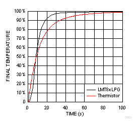
- LMT85LPG(TO-92S 封装)具有快速热时间常量,典型值为 10s(气流速度为 1.2m/s)
- 非常精确:典型值 ±0.4°C
- 1.8V 低压运行
- -8.2mV/°C 的平均传感器增益
- 5.4µA 低静态电流
- 宽温度范围:–50°C 至 150°C
- 输出受到短路保护
- 具有 ±50µA 驱动能力的推挽输出
- 封装尺寸兼容符合行业标准的 LM20/19 和 LM35 温度传感器
- 具有成本优势的热敏电阻替代产品
3 说明
LMT85 是一款高精度 CMOS 温度传感器,其典型精度为 ±0.4°C(最大值为 ±2.7°C),且线性模拟输出电压与温度成反比关系。1.8V 工作电源电压、5.4μA 静态电流和 0.7ms 开通时间可实现有效的功率循环架构,以最大限度地降低无人机和传感器节点等电池供电 应用 的功耗。LMT85LPG 穿孔 TO-92S 封装快速热时间常量支持非板载时间温度敏感型 应用, 例如烟雾和热量探测器。 得益于宽工作范围内的精度和其他 特性, 使得 LMT85 成为热敏电阻的优质替代产品。
对于具有不同平均传感器增益和类似精度的器件,请参阅 类似替代器件 了解 LMT8x 系列中的替代器件。
器件信息(1)
| 器件型号 | 封装 | 封装尺寸(标称值) |
|---|---|---|
| LMT85 | SOT (5) | 2.00mm × 1.25mm |
| TO-92 (3) | 4.30mm × 3.50mm | |
| TO-92S (3) | 4.00mm × 3.15mm |
热时间常量
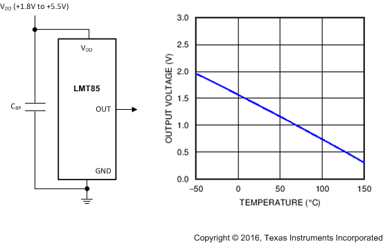
输出电压与温度间的关系
4 修订历史记录
Changes from D Revision (June 2017) to E Revision
- 将汽车器件移到了单独的数据表中 (SNIS200)Go
- Changed TO-92 GND pin number from: 1 to: 3 Go
- Changed TO-92 VDD pin number from: 3 to: 1 Go
Changes from C Revision (October 2015) to D Revision
- 将数据表更新为最新的文档和翻译标准Go
- 将 AEC-Q100 汽车标准项目符号添加到了“特性”中Go
- 添加了时间常量图Go
- 将磁盘驱动器、游戏、无线收发器和手机从“应用”中进行了删除Go
- Added LPG (TO-92S) packageGo
- Added Figure 10 to Typical CharacteristicsGo
Changes from B Revision (May 2014) to C Revision
- Deleted 所有涉及 TO-126 封装的内容Go
- Added TO-92 LPM pin configuration graphicGo
- Changed Handling Ratings to ESD Ratings and moved Storage Temperature to Absolute Maximum Ratings tableGo
- Changed KV to V Go
- Added TO-92 LP and LPM layout recommendationsGo
Changes from A Revision (June 2013) to B Revision
- Changed 更改了数据表流程和布局,以符合 TI 新标准。在整个文档内添加了以下章节:应用范围和实施、电源建议、布局布线、器件和文档支持、机械、封装和可订购信息。Go
- Added 在文档中增加了 TO-92 和 TO-126 封装信息。Go
- Changed from 450°C/W to 275 °C/W. New specification is derived using TI ' s latest methodology. Go
- Changed Temperature Accuracy Conditions from 70°C to 20°C and VDD from 1.9V to 1.8VGo
- Deleted Note: The input current is leakage only and is highest at high temperature. It is typically only 0.001 µA. The 1 µA limit is solely based on a testing limitation and does not reflect the actual performance of the part.Go
5 Device Comparison Tables
Table 1. Available Device Packages
| ORDER NUMBER(1) | PACKAGE | PIN | BODY SIZE (NOM) | MOUNTING TYPE |
|---|---|---|---|---|
| LMT85DCK | SOT (AKA(2): SC70, DCK) | 5 | 2.00 mm × 1.25 mm | Surface Mount |
| LMT85LP | TO-92 (AKA(2): LP) | 3 | 4.30 mm × 3.50 mm | Through-hole; straight leads |
| LMT85LPG | TO-92S (AKA(2): LPG) | 3 | 4.00 mm × 3.15 mm | Through-hole; straight leads |
| LMT85LPM | TO-92 (AKA(2): LPM) | 3 | 4.30 mm × 3.50 mm | Through-hole; formed leads |
| LMT85DCK-Q1 | SOT (AKA(2): SC70, DCK) | 5 | 2.00 mm × 1.25 mm | Surface Mount |
6 Pin Configuration and Functions

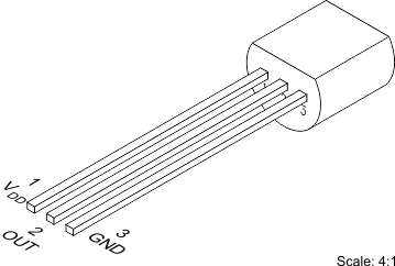
Pin Functions
| PIN | TYPE | DESCRIPTION | ||||
|---|---|---|---|---|---|---|
| NAME | SOT (SC70) | TO-92 | TO-92S | EQUIVALENT CIRCUIT | FUNCTION | |
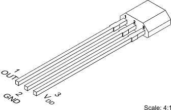
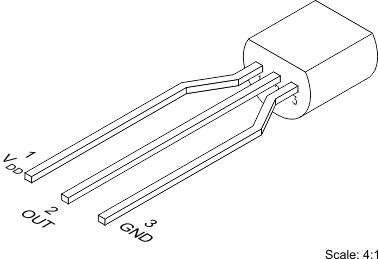
| GND | 2(1) , 5 | 3 | 2 | Ground | N/A | Power Supply Ground |
| OUT | 3 | 2 | 1 | Analog Output |
 |
Outputs a voltage that is inversely proportional to temperature |
| VDD | 1, 4 | 1 | 3 | Power | N/A | Positive Supply Voltage |
7 Specifications
7.1 Absolute Maximum Ratings
See (1)(3)| MIN | MAX | UNIT | ||
|---|---|---|---|---|
| Supply voltage | −0.3 | 6 | V | |
| Voltage at output pin | −0.3 | (VDD + 0.5) | V | |
| Output current | –7 | 7 | mA | |
| Input current at any pin (2) | –5 | 5 | mA | |
| Maximum junction temperature (TJMAX) | 150 | °C | ||
| Storage temperature, Tstg | –65 | 150 | °C | |
7.2 ESD Ratings
| VALUE | UNIT | |||
|---|---|---|---|---|
| LMT85LP in TO-92/TO-92S package | ||||
| V(ESD) | Electrostatic discharge | Human-body model (HBM), per ANSI/ESDA/JEDEC JS-001(1)(3) | ±2500 | V |
| Charged-device model (CDM), per JEDEC specification JESD22-C101(2) | ±1000 | |||
| LMT85DCK in SC70 package | ||||
| V(ESD) | Electrostatic discharge | Human-body model (HBM), per JESD22-A114(3) | ±2500 | V |
| Charged-device model (CDM), per JEDEC specification JESD22-C101(2) | ±1000 | |||
7.3 Recommended Operating Conditions
| MIN | MAX | UNIT | |
|---|---|---|---|
| Specified temperature | TMIN ≤ TA ≤ TMAX | °C | |
| −50 ≤ TA ≤ 150 | °C | ||
| Supply voltage (VDD) | 1.8 | 5.5 | V |
7.4 Thermal Information(1)
| THERMAL METRIC(2) | LMT85/ LMT85-Q1 |
LMT85LP | LMT85LPG | UNIT | |
|---|---|---|---|---|---|
| DCK (SOT/SC70) | LP/LPM (TO-92) | LPG (TO-92S) | |||
| 5 PINS | 3 PINS | 3 PINS | |||
| RθJA | Junction-to-ambient thermal resistance (3)(4) | 275 | 167 | 130.4 | °C/W |
| RθJC(top) | Junction-to-case (top) thermal resistance | 84 | 90 | 64.2 | °C/W |
| RθJB | Junction-to-board thermal resistance | 56 | 146 | 106.2 | °C/W |
| ψJT | Junction-to-top characterization parameter | 1.2 | 35 | 14.6 | °C/W |
| ψJB | Junction-to-board characterization parameter | 55 | 146 | 106.2 | °C/W |
7.5 Accuracy Characteristics
These limits do not include DC load regulation. These stated accuracy limits are with reference to the values in Table 3.| PARAMETER | TEST CONDITIONS | MIN(1) | TYP(2) | MAX(1) | UNIT |
|---|---|---|---|---|---|
| Temperature accuracy (3) | TA = TJ= 20°C to 150°C; VDD = 1.8 V to 5.5 V | –2.7 | ±0.4 | 2.7 | °C |
| TA = TJ= 0°C to 150°C; VDD = 1.9 V to 5.5 V | –2.7 | ±0.7 | 2.7 | °C | |
| TA = TJ= 0°C to 150°C; VDD = 2.6 V to 5.5 V | ±0.3 | °C | |||
| TA = TJ= –50°C to 0°C; VDD = 2.3 V to 5.5 V | –2.7 | ±0.7 | 2.7 | °C | |
| TA = TJ= –50°C to 0°C; VDD = 2.9 V to 5.5 V | ±0.25 | °C |
7.6 Electrical Characteristics
Unless otherwise noted, these specifications apply for VDD = +1.8V to +5.5V. MIN and MAX limits apply for TA = TJ = TMIN to TMAX, unless otherwise noted; typical values apply for TA = TJ = 25°C.| PARAMETER | TEST CONDITIONS | MIN (1) | TYP (2) | MAX (1) | UNIT | ||
|---|---|---|---|---|---|---|---|
| Average sensor gain (output transfer function slope) | –30°C and 90°C used to calculate average sensor gain | –8.2 | mV/°C | ||||
| Load regulation (3) | Source ≤ 50 μA, (VDD - VOUT) ≥ 200 mV | –1 | –0.22 | mV | |||
| Sink ≤ 50 μA, VOUT ≥ 200 mV | 0.26 | 1 | mV | ||||
| Line regulation (4) | 200 | μV/V | |||||
| IS | Supply current | TA = TJ = 30°C to 150°C, (VDD - VOUT) ≥ 100 mV | 5.4 | 8.1 | μA | ||
| TA = TJ = -50°C to 150°C, (VDD - VOUT) ≥ 100 mV | 5.4 | 9 | μA | ||||
| CL | Output load capacitance | 1100 | pF | ||||
| Power-on time (5) | CL= 0 pF to 1100 pF | 0.7 | 1.9 | ms | |||
| Output drive | TA = TJ = 25°C | –50 | +50 | µA | |||
7.7 Typical Characteristics
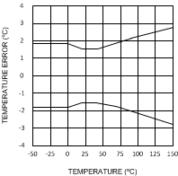 Figure 1. Temperature Error vs Temperature
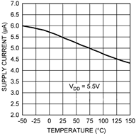 Figure 3. Supply Current vs Temperature
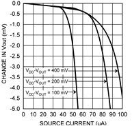 Figure 5. Load Regulation, Sourcing Current
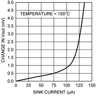
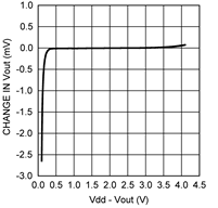 Figure 7. Change in Vout vs Overhead Voltage
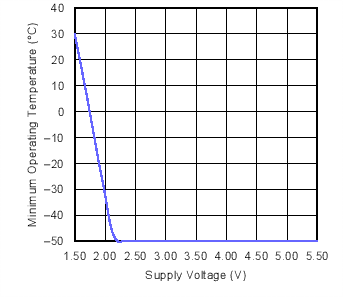
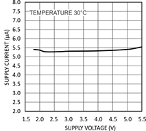
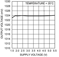 Figure 9. Output Voltage vs Supply Voltage
8 Detailed Description
8.1 Overview
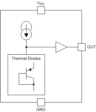
The LMT85 is an analog output temperature sensor. The temperature sensing element is comprised of a simple base emitter junction that is forward biased by a current source. The temperature-sensing element is then buffered by an amplifier and provided to the OUT pin. The amplifier has a simple push-pull output stage thus providing a low impedance output source.
8.2 Functional Block Diagram
Full-Range Celsius Temperature Sensor (−50°C to 150°C).
8.3 Feature Description
8.3.1 LMT85 Transfer Function
The output voltage of the LMT85, across the complete operating temperature range, is shown in Table 3. This table is the reference from which the LMT85 accuracy specifications (listed in the Accuracy Characteristics section) are determined. This table can be used, for example, in a host processor look-up table. A file containing this data is available for download at the LMT85 product folder under Tools and Software Models.
Table 3. LMT85 Transfer Table
| TEMP (°C) |
VOUT
(mV) |
TEMP (°C) |
VOUT
(mV) |
TEMP (°C) |
VOUT
(mV) |
TEMP (°C) |
VOUT
(mV) |
TEMP (°C) |
VOUT
(mV) |
||||
|---|---|---|---|---|---|---|---|---|---|---|---|---|---|
| -50 | 1955 | -10 | 1648 | 30 | 1324 | 70 | 991 | 110 | 651 | ||||
| -49 | 1949 | -9 | 1639 | 31 | 1316 | 71 | 983 | 111 | 642 | ||||
| -48 | 1942 | -8 | 1631 | 32 | 1308 | 72 | 974 | 112 | 634 | ||||
| -47 | 1935 | -7 | 1623 | 33 | 1299 | 73 | 966 | 113 | 625 | ||||
| -46 | 1928 | -6 | 1615 | 34 | 1291 | 74 | 957 | 114 | 617 | ||||
| -45 | 1921 | -5 | 1607 | 35 | 1283 | 75 | 949 | 115 | 608 | ||||
| -44 | 1915 | -4 | 1599 | 36 | 1275 | 76 | 941 | 116 | 599 | ||||
| -43 | 1908 | -3 | 1591 | 37 | 1267 | 77 | 932 | 117 | 591 | ||||
| -42 | 1900 | -2 | 1583 | 38 | 1258 | 78 | 924 | 118 | 582 | ||||
| -41 | 1892 | -1 | 1575 | 39 | 1250 | 79 | 915 | 119 | 573 | ||||
| -40 | 1885 | 0 | 1567 | 40 | 1242 | 80 | 907 | 120 | 565 | ||||
| -39 | 1877 | 1 | 1559 | 41 | 1234 | 81 | 898 | 121 | 556 | ||||
| -38 | 1869 | 2 | 1551 | 42 | 1225 | 82 | 890 | 122 | 547 | ||||
| -37 | 1861 | 3 | 1543 | 43 | 1217 | 83 | 881 | 123 | 539 | ||||
| -36 | 1853 | 4 | 1535 | 44 | 1209 | 84 | 873 | 124 | 530 | ||||
| -35 | 1845 | 5 | 1527 | 45 | 1201 | 85 | 865 | 125 | 521 | ||||
| -34 | 1838 | 6 | 1519 | 46 | 1192 | 86 | 856 | 126 | 513 | ||||
| -33 | 1830 | 7 | 1511 | 47 | 1184 | 87 | 848 | 127 | 504 | ||||
| -32 | 1822 | 8 | 1502 | 48 | 1176 | 88 | 839 | 128 | 495 | ||||
| -31 | 1814 | 9 | 1494 | 49 | 1167 | 89 | 831 | 129 | 487 | ||||
| -30 | 1806 | 10 | 1486 | 50 | 1159 | 90 | 822 | 130 | 478 | ||||
| -29 | 1798 | 11 | 1478 | 51 | 1151 | 91 | 814 | 131 | 469 | ||||
| -28 | 1790 | 12 | 1470 | 52 | 1143 | 92 | 805 | 132 | 460 | ||||
| -27 | 1783 | 13 | 1462 | 53 | 1134 | 93 | 797 | 133 | 452 | ||||
| -26 | 1775 | 14 | 1454 | 54 | 1126 | 94 | 788 | 134 | 443 | ||||
| -25 | 1767 | 15 | 1446 | 55 | 1118 | 95 | 779 | 135 | 434 | ||||
| -24 | 1759 | 16 | 1438 | 56 | 1109 | 96 | 771 | 136 | 425 | ||||
| -23 | 1751 | 17 | 1430 | 57 | 1101 | 97 | 762 | 137 | 416 | ||||
| -22 | 1743 | 18 | 1421 | 58 | 1093 | 98 | 754 | 138 | 408 | ||||
| -21 | 1735 | 19 | 1413 | 59 | 1084 | 99 | 745 | 139 | 399 | ||||
| -20 | 1727 | 20 | 1405 | 60 | 1076 | 100 | 737 | 140 | 390 | ||||
| -19 | 1719 | 21 | 1397 | 61 | 1067 | 101 | 728 | 141 | 381 | ||||
| -18 | 1711 | 22 | 1389 | 62 | 1059 | 102 | 720 | 142 | 372 | ||||
| -17 | 1703 | 23 | 1381 | 63 | 1051 | 103 | 711 | 143 | 363 | ||||
| -16 | 1695 | 24 | 1373 | 64 | 1042 | 104 | 702 | 144 | 354 | ||||
| -15 | 1687 | 25 | 1365 | 65 | 1034 | 105 | 694 | 145 | 346 | ||||
| -14 | 1679 | 26 | 1356 | 66 | 1025 | 106 | 685 | 146 | 337 | ||||
| -13 | 1671 | 27 | 1348 | 67 | 1017 | 107 | 677 | 147 | 328 | ||||
| -12 | 1663 | 28 | 1340 | 68 | 1008 | 108 | 668 | 148 | 319 | ||||
| -11 | 1656 | 29 | 1332 | 69 | 1000 | 109 | 660 | 149 | 310 | ||||
| 150 | 301 |
Although the LMT85 is very linear, its response does have a slight umbrella parabolic shape. This shape is very accurately reflected in Table 3. The Transfer Table can be calculated by using the parabolic equation (Equation 1).

The parabolic equation is an approximation of the transfer table and the accuracy of the equation degrades slightly at the temperature range extremes. Equation 1 can be solved for T resulting in:

For an even less accurate linear transfer function approximation, a line can easily be calculated over the desired temperature range using values from the Table and a two-point equation (Equation 3):

where
- V is in mV,
- T is in °C,
- T1 and V1 are the coordinates of the lowest temperature,
- and T2 and V2 are the coordinates of the highest temperature.
For example, if the user wanted to resolve this equation, over a temperature range of 20°C to 50°C, they would proceed as follows:


Using this method of linear approximation, the transfer function can be approximated for one or more temperature ranges of interest.
8.4 Device Functional Modes
8.4.1 Mounting and Thermal Conductivity
The LMT85 can be applied easily in the same way as other integrated-circuit temperature sensors. It can be glued or cemented to a surface.
To ensure good thermal conductivity, the backside of the LMT85 die is directly attached to the GND pin. The temperatures of the lands and traces to the other leads of the LMT85 will also affect the temperature reading.
Alternatively, the LMT85 can be mounted inside a sealed-end metal tube, and can then be dipped into a bath or screwed into a threaded hole in a tank. As with any IC, the LMT85 and accompanying wiring and circuits must be kept insulated and dry, to avoid leakage and corrosion. This is especially true if the circuit may operate at cold temperatures where condensation can occur. If moisture creates a short circuit from the output to ground or VDD, the output from the LMT85 will not be correct. Printed-circuit coatings are often used to ensure that moisture cannot corrode the leads or circuit traces.
The thermal resistance junction to ambient (RθJA or θJA) is the parameter used to calculate the rise of a device junction temperature due to its power dissipation. Use Equation 7 to calculate the rise in the LMT85 die temperature:

where
- TA is the ambient temperature,
- IS is the supply current,
- ILis the load current on the output,
- and VO is the output voltage.
For example, in an application where TA = 30°C, VDD = 5 V, IS = 5.4 μA, VOUT = 1324 mV, and IL = 2 μA, the junction temperature would be 30.014°C, showing a self-heating error of only 0.014°C. Because the junction temperature of the LMT85 is the actual temperature being measured, take care to minimize the load current that the LMT85 is required to drive. Thermal Information shows the thermal resistance of the LMT85.
8.4.2 Output and Noise Considerations
A push-pull output gives the LMT85 the ability to sink and source significant current. This is beneficial when, for example, driving dynamic loads like an input stage on an analog-to-digital converter (ADC). In these applications the source current is required to quickly charge the input capacitor of the ADC. The LMT85 device is ideal for this and other applications which require strong source or sink current.
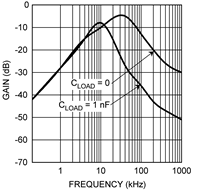
The LMT85 supply-noise gain (the ratio of the AC signal on VOUT to the AC signal on VDD) was measured during bench tests. The typical attenuation is shown in Figure 8 found in the Typical Characteristics. A load capacitor on the output can help to filter noise.
For operation in very noisy environments, some bypass capacitance should be present on the supply within approximately 5 centimeters of the LMT85.
8.4.3 Capacitive Loads
The LMT85 handles capacitive loading well. In an extremely noisy environment, or when driving a switched sampling input on an ADC, it may be necessary to add some filtering to minimize noise coupling. Without any precautions, the LMT85 can drive a capacitive load less than or equal to 1100 pF as shown in Figure 11. For capacitive loads greater than 1100 pF, a series resistor may be required on the output, as shown in Figure 12.
 Figure 11. LMT85 No Decoupling Required for Capacitive Loads Less Than 1100 pF
 Figure 12. LMT85 with Series Resistor for Capacitive Loading Greater Than 1100 pF
Table 4. Recommended Series Resistor Values
| CLOAD | MINIMUM RS |
|---|---|
| 1.1 nF to 99 nF | 3 kΩ |
| 100 nF to 999 nF | 1.5 kΩ |
| 1 μF | 800 Ω |
8.4.4 Output Voltage Shift
The LMT85 is very linear over temperature and supply voltage range. Due to the intrinsic behavior of an NMOS/PMOS rail-to-rail buffer, a slight shift in the output can occur when the supply voltage is ramped over the operating range of the device. The location of the shift is determined by the relative levels of VDD and VOUT. The shift typically occurs when VDD- VOUT = 1 V.
This slight shift (a few millivolts) takes place over a wide change (approximately 200 mV) in VDD or VOUT. Because the shift takes place over a wide temperature change of 5°C to 20°C, VOUT is always monotonic. The accuracy specifications in the Accuracy Characteristics table already include this possible shift.
9 Application and Implementation
NOTE
Information in the following applications sections is not part of the TI component specification, and TI does not warrant its accuracy or completeness. TI’s customers are responsible for determining suitability of components for their purposes. Customers should validate and test their design implementation to confirm system functionality.
9.1 Application Information
The LMT85 features make it suitable for many general temperature-sensing applications. It can operate down to 1.8-V supply with 5.4-µA power consumption, making it ideal for battery powered devices. Package options like the through-hole TO-92 package allow the LMT85 to be mounted onboard, off-board, to a heat sink, or on multiple unique locations in the same application.
9.2 Typical Applications
9.2.1 Connection to an ADC
 Figure 13. Suggested Connection to a Sampling Analog-to-Digital Converter Input Stage
9.2.1.1 Design Requirements
Most CMOS ADCs found in microcontrollers and ASICs have a sampled data comparator input structure. When the ADC charges the sampling cap, it requires instantaneous charge from the output of the analog source such as the LMT85 temperature sensor and many op amps. This requirement is easily accommodated by the addition of a capacitor (CFILTER).
9.2.1.2 Detailed Design Procedure
The size of CFILTER depends on the size of the sampling capacitor and the sampling frequency. Because not all ADCs have identical input stages, the charge requirements will vary. This general ADC application is shown as an example only.
9.2.1.3 Application Curve
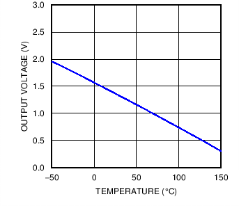 Figure 14. Analog Output Transfer Function
9.2.2 Conserving Power Dissipation With Shutdown
 Figure 15. Simple Shutdown Connection of the LMT85
9.2.2.1 Design Requirements
Because the power consumption of the LMT85 is less than 9 µA, it can simply be powered directly from any logic gate output and therefore not require a specific shutdown pin. The device can even be powered directly from a micro controller GPIO. In this way, it can easily be turned off for cases such as battery-powered systems where power savings are critical.
9.2.2.2 Detailed Design Procedure
Simply connect the VDD pin of the LMT85 directly to the logic shutdown signal from a microcontroller.
9.2.2.3 Application Curves
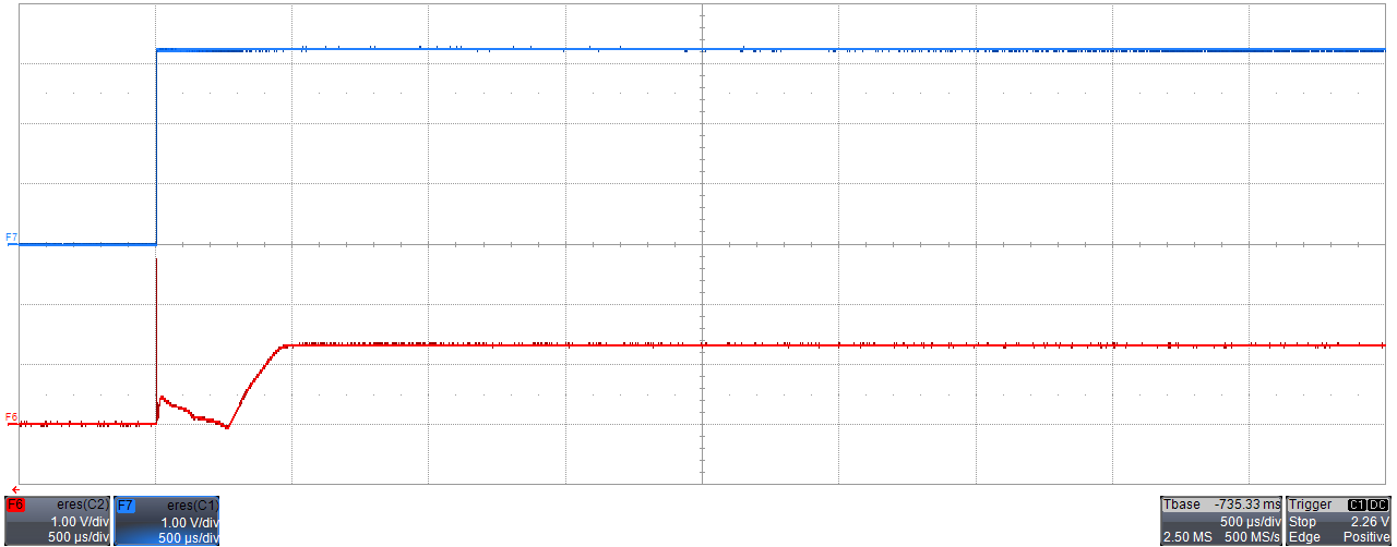
INDENT:
Time: 500 µs/div; Top Trace: VDD 1 V/div;Bottom Trace: OUT 1 V/div
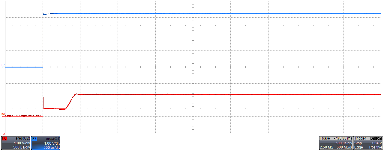
INDENT:
Time: 500 µs/div; Top trace: VDD 1V/div;Bottom trace: OUT 1 V/div
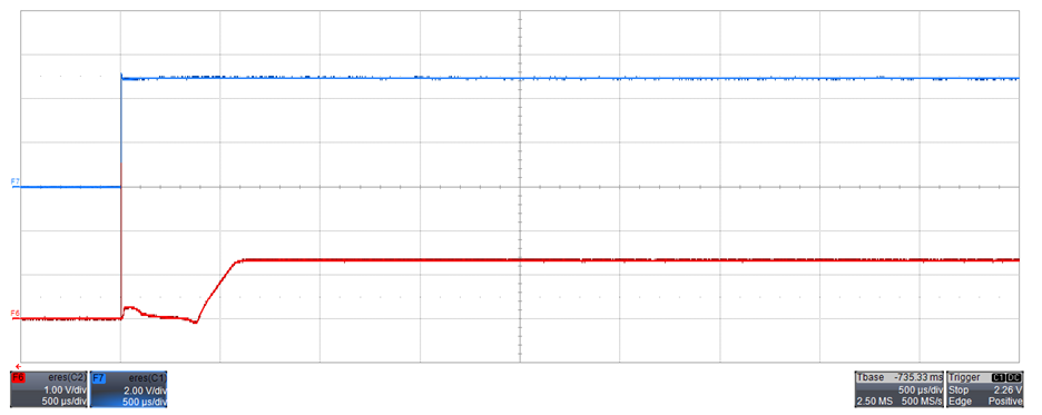
INDENT:
Time: 500 µs/div; Top trace: VDD 2 V/div;Bottom trace: OUT 1 V/div
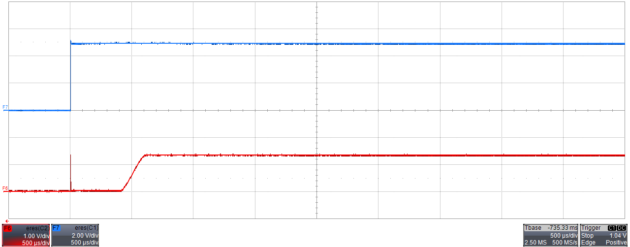
INDENT:
Time: 500 µs/div; Top trace: VDD 2 V/div;Bottom trace: OUT 1 V/div
10 Power Supply Recommendations
The low supply current and supply range (1.8 V to 5.5 V) of the LMT85 allow the device to easily be powered from many sources. Power supply bypassing is optional and is mainly dependent on the noise on the power supply used. In noisy systems it may be necessary to add bypass capacitors to lower the noise that is coupled to the output of the LMT85.
