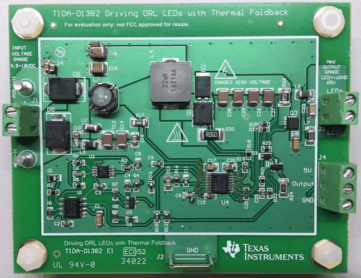
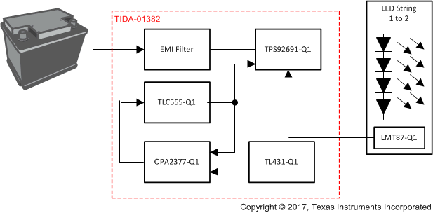
The TIDA-01382 implements thermal foldback for derating current through the LEDs without using a microcontroller. This TI Design uses the following devices: the TPS92691-Q1 multi-topology LED driver in boost configuration to control the LEDs, the TLC555-Q1 LinCMOS™ timer together with the OPA2377-Q1 operational amplifier to measure and generate the accurate PWM signal by applying a feedback loop and a precision shunt regulator for setting the accurate duty cycle, and the LMT87-Q1 to implement thermal foldback. The input and output stage of the design is EMI- and EMC-filtered and can be directly supplied by a car battery.
TIDA-01382 | Design Folder |
TPS92691-Q1 | Product Folder |
LMT87-Q1 | Product Folder |
TLC555-Q1 | Product Folder |
OPA2377-Q1 | Product Folder |
TL431A-Q1 | Product Folder |
![]() |
An IMPORTANT NOTICE at the end of this TI reference design addresses authorized use, intellectual property matters and other important disclaimers and information. |
This system has been designed to be a solution to precision pulse width modulation (PWM) dimming daytime running lights and implement thermal foldback without the necessity of using a microcontroller (MCU). The design includes key peripherals like electromagnetic interference (EMI) and electromagnetic compatibility (EMC) filtering voltage conditioning (shunt regulator), thermal foldback, precision clock generation, and LED drive.
The TIDA-01382 has been designed with the following points in consideration:
PARAMETER | COMMENTS | MIN | TYP | MAX | UNIT | |
---|---|---|---|---|---|---|
SYSTEM INPUT AND OUTPUT | ||||||
VIN | Operating input voltage | Battery-voltage range; outputs are functional | 5 | 14 | 18 | V |
VUVLO | Input UVLO setting | Undervoltage lockout (UVLO) | — | 4.5 | — | — |
VSWMax | Vmax switch | Maximum switch node voltage | — | — | 100 | V |
VOUT | Output voltage | LED+ to LED– (Boost) | 21 | — | 60 | V |
VOUT | Output voltage | LED + to VIN (Boost-to-Battery) | 3 | — | 36 | — |
VTR | Transient immunity | Load dump (ISO7637-2) | — | — | 60 | V |
VIN_MIN | Minimum input voltage | Cold crank (ISO 7637-2) | 5 | — | — | V |
IIN | Input current | Output at full load | — | 2 | — | A |
IOUT | Output current | Maximum current per string | — | 350 | 365 | mA |
Maximum output power | — | — | — | — | 25 | W |
PWM dimming range | 240-Hz PWM frequency | — | — | 20:1 | — | — |
LEDOpen and short detect | LED open and short detection | — | — | Yes | — | — |
LED Single short detect | LED single-short detection | — | — | No | — | — |
ONBOARD VOLTAGES | ||||||
V 5V5 | Auxiliary supply, shunt regulator | TLC555, LMT87-Q1, op amp supply, and reference generation | — | 5 | — | V |
VCC | Bias | Supply shunt regulator
(TLE431-Q1) |
— | 5 | — | V |
VPREC_PWM | TLC555 out | Amplitude TLC555 clock at output | — | 5 | — | V |
CLOCKS | ||||||
fPREC_PWM | Square wave frequency | Frequency at TLC555-Q1 out, U1 | 240 | — | — | Hz |
DOUT | Square wave duty cycle | Duty cycle of fPREC_PWM | 5 | — | 50 | % |
DACC | Duty cycle accuracy | Accuracy of DOUT | 2% | — | — | — |
fOSCL | Oscillator frequency | LED driver, TPS92691-Q1 | — | 390 | — | kHz |
THERMAL | ||||||
TA | Temperature range | Operating and ambient temperature | –40 | — | 125 | °C |
PULSE TOLERANCE | ||||||
Cold crank | Operational | |||||
Jump start | Operational | |||||
BASEBOARD | ||||||
Number of layers | Two layers, single-side populated | |||||
Form factor | 71 mm × 51 mm |
The LMT87-Q1 is a precision CMOS integrated-circuit temperature sensor with an analog output voltage that is linearly and inversely proportional to temperature. Its features make it suitable for many general temperature sensing applications. It can operate down to a 2.7-V supply with a 5.4-μA power consumption. Package options including a through-hole TO-92 package allows the LMT87-Q1 to be mounted onboard, off-board, to a heat sink, or on multiple unique locations in the same application. A class-AB output structure gives the LMT87-Q1 a strong output source and sink current capability that can directly drive up to 1.1-nF capacitive loads. This means it is well suited to drive an analog-to-digital converter sample-and-hold input with its transient load requirements. It has accuracy specified in the operating range of −50°C to 150°C. The accuracy, three-lead package options, and other features also make the LMT87-Q1 an alternative to NTC or PTC thermistors
The TLC555 is a monolithic-timing circuit fabricated using the TI LinCMOS process (see Figure 3). The timer is fully compatible with CMOS, TTL, and MOS logic and operates at frequencies up to 2 MHz. Because of the high input impedance of this device, it uses smaller timing capacitors than those used by the NE555 device. As a result, more accurate time delays and oscillations are possible. Power consumption is low across the full range of power-supply voltage. The advantage of the TLC555-Q1 is that it exhibits greatly reduced supply-current spikes during output transitions. Although the CMOS output is capable of sinking over 100 mA and sourcing over 10 mA, the main reason the TLC555-Q1 is able to have low current spikes is because of its edge rates. This feature minimizes the requirement for the large decoupling capacitors required by the NE555.
The OPA2377-Q1 is a wide-bandwidth CMOS amplifier that provides very low noise, low input bias current, and low offset voltage while operating on a low quiescent current of 0.76 mA (typical).
The OPA2377-Q1 operational amplifier (op amp) is optimized for low voltage, single-supply applications. The exceptional combination of AC and DC performance makes the device ideal for a wide range of applications, including small signal conditioning and active filters. In addition, this part has a wide supply range with excellent power supply rejection ratio (PSRR), which makes it appealing for applications that run directly from batteries without regulation.
Figure 4 shows a block diagram of the OPA2377-Q1 op amp.
The TL431-Q1 is a three-terminal adjustable shunt regulator with specified thermal stability over applicable automotive temperature ranges (see Figure 5). The output voltage can be set to any value between VREF (approximately 2.5 V) and 36 V, with two external resistors. This device has a typical output impedance of 0.2 Ω. Active output circuitry provides a sharp turnon characteristic, making this device an excellent replacement for Zener diodes in many applications, such as onboard regulation, adjustable power supplies, and switching power supplies.
The TPS92691-Q1 is a versatile LED controller that can support a range of step-up or step-down driver topologies (see Figure 6). The device implements a fixed-frequency, peak-current-mode control technique with programmable switching frequency, slope compensation, and soft-start timing. The device incorporates a high-voltage (65-V) rail-to-rail current sense amplifier that can directly measure LED current using either a high-side or a low-side series sense resistor. The amplifier is designed to achieve low input offset voltage and attain better than ±3% LED current accuracy over a junction temperature range of 25°C to 140°C and output common-mode voltage range of 0 to 60 V.
LED current can be independently modulated using either analog or PWM dimming techniques. A linear analog dimming response with a 15:1 range is obtainable by varying the voltage from 140 mV to 2.25 V across the high impedance analog adjust (IADJ) input. PWM dimming of LED current can be achieved by modulating the PWM input pin with the desired duty cycle and frequency. Use the DDRV gate driver output to enable series FET dimming functionality to obtain over a 1000:1 contrast ratio.
The TPS92691-Q1 supports continuous LED status check through the current monitor (IMON) output. This feature allows for LED short circuit or open circuit detection and protection. Additional fault protection features include VCC UVLO, output OVP, switch cycle-by-cycle current limit, and thermal protection.
This TI Design is not intended to fit any particular form factor. The specific and primary objective of the design with regards to the PCB is to make a solution that is compact, while still providing a way to test the performance of the board. Figure 7 shows a 3D rendering of the board.
In a final-production version of this TI Design, several techniques may be used to reduce the size of the solution: