LP2998/LP2998-Q1 DDR Termination Regulator
1 Features
- AEC-Q100 Test Guidance with the following results (SO PowerPAD-8):
- Device HBM ESD Classification Level H1C
- Junction Temperature Range –40°C to 125°C
- 1.35 V Minimum VDDQ
- Source and Sink Current
- Low Output Voltage Offset
- No External Resistors Required
- Linear Topology
- Suspend to Ram (STR) Functionality
- Low External Component Count
- Thermal Shutdown
2 Applications
- DDR1, DDR2, DDR3, and DDR3L Termination Voltage
- Automotive Infotainment
- FPGA
- Industrial/Medical PC
- SSTL-18, SSTL-2, and SSTL-3 Termination
- HSTL Termination
3 Description
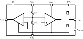
The LP2998 linear regulator is designed to meet JEDEC SSTL-2 and JEDEC SSTL-18 specifications for termination of DDR-SDRAM and DDR2 memory. The device also supports DDR3 and DDR3L VTT bus termination with VDDQ min of 1.35 V. The device contains a high-speed operational amplifier to provide excellent response to load transients. The output stage prevents shoot through while delivering 1.5 A continuous current and transient peaks up to 3 A in the application as required for DDR-SDRAM termination. The LP2998 also incorporates a VSENSE pin to provide superior load regulation and a VREF output as a reference for the chipset and DIMMs.
An additional feature found on the LP2998 is an active low shutdown (SD) pin that provides Suspend To RAM (STR) functionality. When SD is pulled low the VTT output will tri-state providing a high impedance output, but, VREF will remain active. A power savings advantage can be obtained in this mode through lower quiescent current.
Device Information(1)
| PART NUMBER | PACKAGE | BODY SIZE (NOM) |
|---|---|---|
| LP2998 | SO PowerPAD™ (8) | 4.89 mm x 3.90 mm |
| LP2998 | SOIC (8) | 4.90 mm x 3.91 mm |
| LP2998-Q1 | SO PowerPAD™ (8) | 4.89 mm x 3.90 mm |
- For all available packages, see the orderable addendum at the end of the datasheet.
4 Simplified Schematic
5 Revision History
Changes from J Revision (December 2013) to K Revision
- Added DDR3 support throughout datasheetGo
- Changed formatting to match new TI datasheet guidelines; added Device Information and Handling Ratings tables, Power Supply, Layout Examples, and Device and Documentation Support sections; reformatted Detailed Description and Application and Implementation sections. Go
- Changed Electrical Char table condition statement Go
Changes from I Revision (April 2013) to J Revision
6 Pin Configuration and Functions
Pin Functions
| PIN | ||
|---|---|---|
| NUMBER | TYPE | DESCRIPTION |
| 1 | GND | Ground |
| 2 | SD | Shutdown |
| 3 | VSENSE | Feedback pin for regulating VTT. |
| 4 | VREF | Buffered internal reference voltage of VDDQ/2 |
| 5 | VDDQ | Input for internal reference equal to VDDQ/2 |
| 6 | AVIN | Analog input pin |
| 7 | PVIN | Power input pin |
| 8 | VTT | Output voltage for connection to termination resistors |
| EP | Exposed pad thermal connection. Connect to Ground. | |
6.1 Pin Descriptions
| AVIN AND PVIN | AVIN and PVIN are the input supply pins for the LP2998. AVIN is used to supply all the internal control circuitry. PVIN, however, is used exclusively to provide the rail voltage for the output stage used to create VTT. These pins have the capability to work off separate supplies depending on the application. Higher voltages on PVIN will increase the maximum continuous output current because of output RDSON limitations at voltages close to VTT. The disadvantage of high values of PVIN is that the internal power loss will also increase, thermally limiting the design. For SSTL-2 applications, a good compromise would be to connect the AVIN and PVIN directly together at 2.5 V. This eliminates the need for bypassing the two supply pins separately. The only limitation on input voltage selection is that PVIN must be equal to or lower than AVIN. It is recommended to connect PVIN to voltage rails equal to or less than 3.3 V to prevent the thermal limit from tripping because of excessive internal power dissipation. If the junction temperature exceeds the thermal shutdown than the part will enter a shutdown state identical to the manual shutdown where VTT is tri-stated and VREF remains active. |
| VDDQ | VDDQ is the input used to create the internal reference voltage for regulating VTT. The reference voltage is generated from a resistor divider of two internal 50 kΩ resistors. This ensures that VTT will track VDDQ / 2 precisely. The optimal implementation of VDDQ is as a remote sense. This can be achieved by connecting VDDQ directly to the 2.5 V rail at the DIMM instead of AVIN and PVIN. This ensures that the reference voltage tracks the DDR memory rails precisely without a large voltage drop from the power lines. For SSTL-2 applications VDDQ will be a 2.5 V signal, which will create a 1.25 V termination voltage at VTT (See Electrical Characteristics Table for exact values of VTT over temperature). |
|
VSENSE |
The purpose of the sense pin is to provide improved remote load regulation. In most motherboard applications the termination resistors will connect to VTT in a long plane. If the output voltage was regulated only at the output of the LP2998 then the long trace will cause a significant IR drop resulting in a termination voltage lower at one end of the bus than the other. The VSENSE pin can be used to improve this performance, by connecting it to the middle of the bus. This will provide a better distribution across the entire termination bus. If remote load regulation is not used then the VSENSE pin must still be connected to VTT. Care should be taken when a long VSENSE trace is implemented in close proximity to the memory. Noise pickup in the VSENSE trace can cause problems with precise regulation of VTT. A small 0.1 uF ceramic capacitor placed next to the VSENSE pin can help filter any high frequency signals and preventing errors. |
| SHUTDOWN | The LP2998 contains an active low shutdown pin that can be used to tri-state VTT. During shutdown VTT should not be exposed to voltages that exceed AVIN. With the shutdown pin asserted low the quiescent current of the LP2998 will drop, however, VDDQ will always maintain its constant impedance of 100 kΩ for generating the internal reference. Therefore, to calculate the total power loss in shutdown both currents need to be considered. For more information refer to the Thermal Dissipation section. The shutdown pin also has an internal pull-up current, therefore to turn the part on the shutdown pin can either be connected to AVIN or left open. |
| VREF | VREF provides the buffered output of the internal reference voltage VDDQ / 2. This output should be used to provide the reference voltage for the Northbridge chipset and memory. Since these inputs are typically an extremely high impedance, there should be little current drawn from VREF. For improved performance, an output bypass capacitor can be used, located close to the pin, to help with noise. A ceramic capacitor in the range of 0.1 µF to 0.01 µF is recommended. This output remains active during the shutdown state and thermal shutdown events for the suspend to RAM functionality. |
| VTT | VTT is the regulated output that is used to terminate the bus resistors. It is capable of sinking and sourcing current while regulating the output precisely to VDDQ / 2. The LP2998 is designed to handle peak transient currents of up to ± 3 A with a fast transient response. The maximum continuous current is a function of VIN and can be viewed in the Typical Characteristics section. If a transient is expected to last above the maximum continuous current rating for a significant amount of time then the output capacitor should be sized large enough to prevent an excessive voltage drop. Despite the fact that the LP2998 is designed to handle large transient output currents it is not capable of handling these for long durations, under all conditions. The reason for this is the standard packages are not able to thermally dissipate the heat as a result of the internal power loss. If large currents are required for longer durations, then care should be taken to ensure that the maximum junction temperature is not exceeded. Proper thermal derating should always be used (please refer to the Thermal Dissipation section). If the junction temperature exceeds the thermal shutdown point than VTT will tri-state until the part returns below the hysteretic trip-point. |
7 Specifications
7.1 Absolute Maximum Ratings (1)(2)
over operating free-air temperature range (unless otherwise noted)| MIN | MAX | UNIT | |
|---|---|---|---|
| AVIN to GND | −0.3 | 6 | V |
| PVIN to GND | –0.3 | AVIN | V |
| VDDQ(3) | −0.3 | 6 | V |
| Junction temperature | 150 | °C | |
| Lead temperature (soldering, 10 sec) | 260 | °C |
7.2 Handling Ratings: LP2998
| MIN | MAX | UNIT | |||
|---|---|---|---|---|---|
| Tstg | Storage temperature range | −65 | 150 | °C | |
| V(ESD) | Electrostatic discharge | Human body model (HBM), per ANSI/ESDA/JEDEC JS-001, all pins(1) | −1000 | 1000 | V |
7.3 Handling Ratings: LP2998-Q1
| MIN | MAX | UNIT | ||||
|---|---|---|---|---|---|---|
| Tstg | Storage temperature range | −65 | 150 | °C | ||
| V(ESD) | Electrostatic discharge | Human body model (HBM), per AEC Q100-002(1) | −1000 | 1000 | V | |
7.4 Recommended Operating Conditions
over operating free-air temperature range (unless otherwise noted)| MIN | NOM | MAX | UNIT | ||
|---|---|---|---|---|---|
| Junction temperature(1) | –40 | 125 | °C | ||
| AVIN to GND | 2.2 | 5.5 | V | ||
| PVIN supply voltage | 0 | AVIN | V | ||
| SD input voltage | 0 | AVIN | V | ||
7.5 Thermal Information
| THERMAL METRIC(1) | LP2998/LP2998-Q1 | LP2998 | UNIT | |
|---|---|---|---|---|
| SO PowerPAD | SOIC | |||
| 8 PINS | 8 PINS | |||
| RθJA | Junction-to-ambient thermal resistance | 43 | 151 | °C/W |
7.6 Electrical Characteristics
Typical limits tested at TJ = 25°C. Minimum and maximum limits apply over the full operating junction temperature range (TJ = –40°C to 125°C).(2) Unless otherwise specified, AVIN = PVIN = 2.5 V, VDDQ = 2.5 V.(3)| PARAMETER | TEST CONDITIONS | MIN | TYP | MAX | UNIT | |
|---|---|---|---|---|---|---|
| VREF | VREF voltage (DDR I) | VIN = VDDQ = 2.3 V | 1.135 | 1.158 | 1.185 | V |
| VIN = VDDQ = 2.5 V | 1.235 | 1.258 | 1.285 | |||
| VIN = VDDQ = 2.7 V | 1.335 | 1.358 | 1.385 | |||
| VREF voltage (DDR II) | PVIN = VDDQ = 1.7 V | 0.837 | 0.860 | 0.887 | ||
| PVIN = VDDQ = 1.8 V | 0.887 | 0.910 | 0.937 | |||
| PVIN = VDDQ = 1.9 V | 0.936 | 0.959 | 0.986 | |||
| VREF Voltage (DDR III) | PVIN = VDDQ = 1.35V | 0.669 | 0.684 | 0.699 | ||
| PVIN = VDDQ = 1.5V | 0.743 | 0.758 | 0.773 | |||
| PVIN = VDDQ = 1.6V | 0.793 | 0.808 | 0.823 | |||
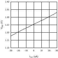
| ZVREF | VREF Output Impedance | IREF = –30 to 30 µA | 2.5 | kΩ | ||
| VTT | VTT Output Voltage (DDR I) (6) | IOUT = 0 A | V | |||
| VIN = VDDQ = 2.3 V | 1.120 | 1.159 | 1.190 | |||
| VIN = VDDQ = 2.5 V | 1.210 | 1.259 | 1.290 | |||
| VIN = VDDQ = 2.7 V | 1.320 | 1.359 | 1.390 | |||
| IOUT = ±1.5 A | ||||||
| VIN = VDDQ = 2.3 V | 1.125 | 1.159 | 1.190 | |||
| VIN = VDDQ = 2.5 V | 1.225 | 1.259 | 1.290 | |||
| VIN = VDDQ = 2.7 V | 1.325 | 1.359 | 1.390 | |||
| VTT Output Voltage (DDR II) (6) | IOUT = 0 A, AVIN = 2.5 V | V | ||||
| PVIN = VDDQ = 1.7 V | 0.822 | 0.856 | 0.887 | |||
| PVIN = VDDQ = 1.8 V | 0.874 | 0.908 | 0.939 | |||
| PVIN = VDDQ = 1.9 V | 0.923 | 0.957 | 0.988 | |||
| IOUT = ±0.5A, AVIN = 2.5 V | ||||||
| PVIN = VDDQ = 1.7 V | 0.820 | 0.856 | 0.890 | |||
| PVIN = VDDQ = 1.8 V | 0.870 | 0.908 | 0.940 | |||
| PVIN = VDDQ = 1.9 V | 0.920 | 0.957 | 0.990 | |||
| VTT Output Voltage (DDR III) (6) | IOUT = 0A, AVIN = 2.5 V | V | ||||
| PVIN = VDDQ = 1.35V | 0.656 | 0.677 | 0.698 | |||
| PVIN = VDDQ = 1.5 V | 0.731 | 0.752 | 0.773 | |||
| PVIN = VDDQ = 1.6 V | 0.781 | 0.802 | 0.823 | |||
| IOUT = 0.2 A, AVIN = 2.5V PVIN = VDDQ = 1.35V |
0.667 | 0.688 | 0.710 | |||
| IOUT = -0.2A, AVIN = 2.5V PVIN = VDDQ = 1.35V |
0.641 | 0.673 | 0.694 | |||
| IOUT = 0.4 A, AVIN = 2.5 V PVIN = VDDQ = 1.5 V |
0.740 | 0.763 | 0.786 | |||
| IOUT = –0.4 A, AVIN = 2.5 V PVIN = VDDQ = 1.5 V |
0.731 | 0.752 | 0.773 | |||
| IOUT = 0.5 A, AVIN = 2.5 V PVIN = VDDQ = 1.6 V |
0.790 | 0.813 | 0.836 | |||
| IOUT = –0.5 A, AVIN = 2.5 V PVIN = VDDQ = 1.6 V |
0.781 | 0.802 | 0.823 | |||
| VOSVtt | VTT Output Voltage Offset (VREF – VTT) for DDR I (6) | IOUT = 0 A | –30 | 0 | 30 | mV |
| IOUT = –1.5 A | –30 | 0 | 30 | |||
| IOUT = 1.5 A | –30 | 0 | 30 | |||
| VTT Output Voltage Offset (VREF – VTT) for DDR II (6) | IOUT = 0 A | –30 | 0 | 30 | ||
| IOUT = –0.5 A | –30 | 0 | 30 | |||
| IOUT = 0.5 A | –30 | 0 | 30 | |||
| VTT Output Voltage Offset (VREF – VTT) for DDR III (6) | IOUT = 0 A | –30 | 0 | 30 | ||
| IOUT = ±0.2 A | –30 | 0 | 30 | |||
| IOUT = ±0.4 A | –30 | 0 | 30 | |||
| IOUT = ±0.5 A | –30 | 0 | 30 | |||
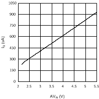
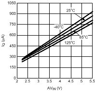
| IQ | Quiescent Current (4) | IOUT = 0 A | 320 | 500 | µA | |
| ZVDDQ | VDDQ Input Impedance | 100 | kΩ | |||
| ISD | Quiescent current in shutdown (4) | SD = 0 V | 115 | 150 | µA | |
| IQ_SD | Shutdown leakage current | SD = 0 V | 2 | 5 | ||
| VIH | Minimum Shutdown High Level | 1.9 | V | |||
| VIL | Maximum Shutdown Low Level | 0.8 | ||||
| Iv | VTT leakage current in shutdown | SD = 0 V VTT = 1.25 V |
1 | 10 | µA | |
| ISENSE | VSENSE Input current | 13 | nA | |||
| TSD | Thermal Shutdown (5) | 165 | °C | |||
| TSD_HYS | Thermal Shutdown Hysteresis | 10 | ||||
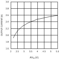
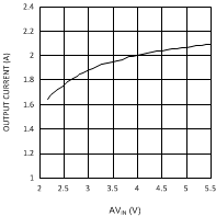
7.7 Typical Characteristics
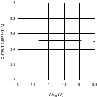
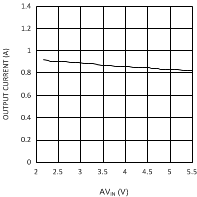
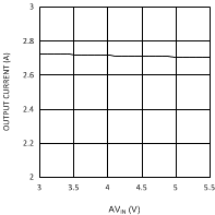
Unless otherwise specified AVIN = PVIN = 2.5 V.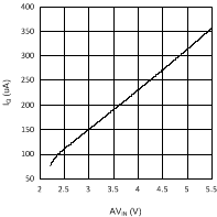
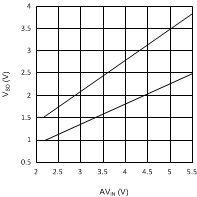
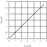
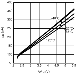
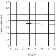
| VDDQ = 2.5 V | PVIN = 1.8 V | |
| VDDQ = 2.5 V | PVIN = 3.3 V | |
| VDDQ = 1.8 V | PVIN = 1.8 V | |
| VDDQ = 1.8 V | PVIN = 3.3 V | |||
8 Detailed Description
8.1 Overview
The LP2998 linear regulator is designed to meet JEDEC SSTL-2 and JEDEC SSTL-18 specifications for termination of DDR-SDRAM and DDR2 memory. The device also supports DDR3 and DDR3L VTT bus termination with VDDQ min of 1.35 V. The device contains a high-speed operational amplifier to provide excellent response to load transients. The output stage prevents shoot through while delivering 1.5 A continuous current and transient peaks up to 3 A in the application as required for DDR-SDRAM termination.
8.2 Functional Block Diagram
8.3 Feature Description
The LP2998 is a linear bus termination regulator designed to meet the JEDEC requirements of SSTL-2 and SSTL-18. The output, VTT is capable of sinking and sourcing current while regulating the output voltage equal to VDDQ / 2. The output stage has been designed to maintain excellent load regulation while preventing shoot through. The LP2998 also incorporates two distinct power rails that separates the analog circuitry from the power output stage. This allows a split rail approach to be utilized to decrease internal power dissipation. It also permits the LP2998 to provide a termination solution for DDR3-SDRAM and DDR3L-SDRAM memory.
8.4 Device Functional Modes
The LP2998 can also be used to provide a termination voltage for other logic schemes such as SSTL-3 or HSTL. Series Stub Termination Logic (SSTL) was created to improve signal integrity of the data transmission across the memory bus. This termination scheme is essential to prevent data error from signal reflections while transmitting at high frequencies encountered with DDR-SDRAM. The most common form of termination is Class II single parallel termination. This involves one RS series resistor from the chipset to the memory and one RT termination resistor. Typical values for RS and RT are 25 Ω, although these can be changed to scale the current requirements from the LP2998. This implementation can be seen below in Figure 16.
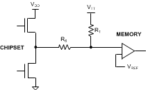 Figure 16. SSTL-Termination Scheme
9 Application and Implementation
9.1 Application Information
9.1.1 Input Capacitor
The LP2998 does not require a capacitor for input stability, but it is recommended for improved performance during large load transients to prevent the input rail from dropping. The input capacitor should be located as close as possible to the PVIN pin. Several recommendations exist dependent on the application required. A typical value recommended for AL electrolytic capacitors is 50 µF. Ceramic capacitors can also be used, a value in the range of 10 µF with X5R or better would be an ideal choice. The input capacitance can be reduced if the LP2998 is placed close to the bulk capacitance from the output of the 2.5 V DC-DC converter. If the two supply rails (AVIN and PVIN) are separated then the 47 uF capacitor should be placed as close to possible to the PVIN rail. An additional 0.1 uF ceramic capacitor can be placed on the AVIN rail to prevent excessive noise from coupling into the device.
9.1.2 Output Capacitor
The LP2998 has been designed to be insensitive of output capacitor size or ESR (Equivalent Series Resistance). This allows the flexibility to use any capacitor desired. The choice for output capacitor will be determined solely on the application and the requirements for load transient response of VTT. As a general recommendation the output capacitor should be sized above 100 µF with a low ESR for SSTL applications with DDR-SDRAM. The value of ESR should be determined by the maximum current spikes expected and the extent at which the output voltage is allowed to droop. Several capacitor options are available on the market and a few of these are highlighted below:
AL - It should be noted that many aluminum electrolytics only specify impedance at a frequency of 120 Hz, which indicates they have poor high frequency performance. Only aluminum electrolytics that have an impedance specified at a higher frequency (between 20 kHz and 100 kHz) should be used for the LP2998. To improve the ESR several AL electrolytics can be combined in parallel for an overall reduction. An important note to be aware of is the extent at which the ESR will change over temperature. Aluminum electrolytic capacitors can have their ESR rapidly increase at cold temperatures.
Ceramic - Ceramic capacitors typically have a low capacitance, in the range of 10 to 100 µF range, but they have excellent AC performance for bypassing noise because of very low ESR (typically less than 10 mΩ). However, some dielectric types do not have good capacitance characteristics as a function of voltage and temperature. Because of the typically low value of capacitance it is recommended to use ceramic capacitors in parallel with another capacitor such as an aluminum electrolytic. A dielectric of X5R or better is recommended for all ceramic capacitors.
Hybrid - Several hybrid capacitors such as OS-CON and SP are available from several manufacturers. These offer a large capacitance while maintaining a low ESR. These are the best solution when size and performance are critical, although their cost is typically higher than any other capacitor.
9.1.3 Thermal Dissipation
Since the LP2998 is a linear regulator any current flow from VTT will result in internal power dissipation generating heat. To prevent damaging the part from exceeding the maximum allowable junction temperature, care should be taken to derate the part dependent on the maximum expected ambient temperature and power dissipation. The maximum allowable internal temperature rise (TRmax) can be calculated given the maximum ambient temperature (TAmax) of the application and the maximum allowable junction temperature (TJmax).
From this equation, the maximum power dissipation (PDmax) of the part can be calculated:
The RθJA of the LP2998 will be dependent on several variables: the package used; the thickness of copper; the number of vias and the airflow.
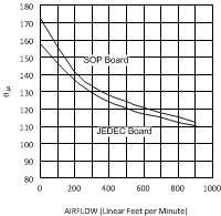 Figure 17. RθJA vs Airflow (SOIC-8)
Additional improvements can be made by the judicious use of vias to connect the part and dissipate heat to an internal ground plane. Using larger traces and more copper on the top side of the board can also help. With careful layout it is possible to reduce the RθJA further than the nominal values shown in Figure 17.
Layout is also extremely critical to maximize the output current with the SO PowerPAD package. By simply placing vias under the DAP the θJA can be lowered significantly.
Additional improvements in lowering the RθJA can also be achieved with a constant airflow across the package. Maintaining the same conditions as above and utilizing the 2x2 via array, Figure 18 shows how the RθJA varies with airflow.
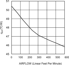 Figure 18. RΘJA vs Airflow Speed (Jedec Board with 4 Vias)
Optimizing the R θJA and placing the LP2998 in a section of a board exposed to lower ambient temperature allows the part to operate with higher power dissipation. The internal power dissipation can be calculated by summing the three main sources of loss: output current at VTT, either sinking or sourcing, and quiescent current at AVIN and VDDQ. During the active state (when shutdown is not held low) the total internal power dissipation can be calculated from the following equations:
To calculate the maximum power dissipation at VTT both conditions at VTT need to be examined, sinking, and sourcing current. Although only one equation will add into the total, VTT cannot source and sink current simultaneously.
The power dissipation of the LP2998 can also be calculated during the shutdown state. During this condition the output VTT will tri-state, therefore that term in the power equation will disappear as it cannot sink or source any current (leakage is negligible). The only losses during shutdown will be the reduced quiescent current at AVIN and the constant impedance that is seen at the VDDQ pin.
9.2 Typical Application
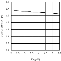
Several different application circuits are shown below to illustrate some of the options that are possible in configuring the LP2998. Graphs of the individual circuit performance can be found in the Typical Characteristics section. These curves illustrate how the maximum output current is affected by changes in AVIN and PVIN.
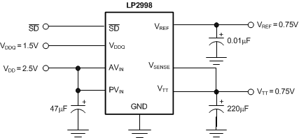 Figure 19. Typical Application Circuit
9.2.1 DDR-III Applications
With the separate VDDQ pin and an internal resistor divider it is possible to use the LP2998 in applications utilizing DDR-III memory. The output stage is connected to the 1.5 V rail and the AVIN pin can be connected to a 2.2 V to 5.5 V rail.
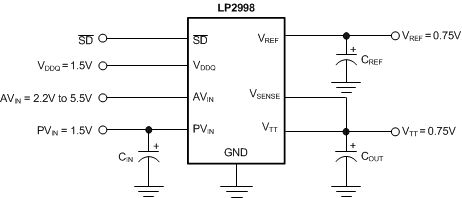 Figure 20. Recommended DDR-III Termination
If it is not desirable to use the 1.5 V - 2.5 V rail it is possible to connect the output stage to a 3.3 V rail. Care should be taken to not exceed the maximum junction temperature as the thermal dissipation increases with lower VTT output voltages. For this reason it is not recommended to power PVIN off a rail higher than the nominal 3.3 V. The advantage of this configuration is that it has the ability to source and sink a higher maximum continuous current.
9.2.2 DDR-II Applications
With the separate VDDQ pin and an internal resistor divider it is possible to use the LP2998 in applications utilizing DDR-II memory. Figure 21 and Figure 22 show several implementations of recommended circuits with output curves displayed in the Typical Characteristics. Figure 21 shows the recommended circuit configuration for DDR-II applications. The output stage is connected to the 1.8 V rail and the AVIN pin can be connected to either a 3.3 V or 5 V rail.
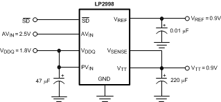 Figure 21. Recommended DDR-II Termination
If it is not desirable to use the 1.8 V rail it is possible to connect the output stage to a 3.3 V rail. Care should be taken to not exceed the maximum junction temperature as the thermal dissipation increases with lower VTT output voltages. For this reason it is not recommended to power PVIN off a rail higher than the nominal 3.3 V. The advantage of this configuration is that it has the ability to source and sink a higher maximum continuous current.
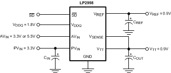 Figure 22. DDR-II Termination with Higher Voltage Rails
9.2.3 SSTL-2 Applications
For the majority of applications that implement the SSTL-2 termination scheme it is recommended to connect all the input rails to the 2.5 V rail. This provides an optimal trade-off between power dissipation and component count and selection. An example of this circuit can be seen in Figure 23.
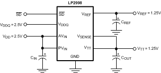 Figure 23. Recommended SSTL-2 Implementation
If power dissipation or efficiency is a major concern then the LP2998 has the ability to operate on split power rails. The output stage (PVIN) can be operated on a lower rail such as 1.8 V and the analog circuitry (AVIN) can be connected to a higher rail such as 2.5 V, 3.3 V, or 5 V. This allows the internal power dissipation to be lowered when sourcing current from VTT. The disadvantage of this circuit is that the maximum continuous current is reduced because of the lower rail voltage, although it is adequate for all motherboard SSTL-2 applications. Increasing the output capacitance can also help if periods of large load transients will be encountered.
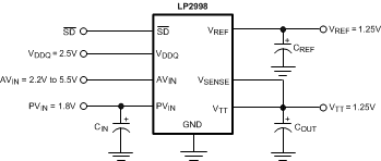 Figure 24. Lower Power Dissipation SSTL-2 Implementation
The third option for SSTL-2 applications in the situation that a 1.8 V rail is not available and it is not desirable to use 2.5 V, is to connect the LP2998 power rail to 3.3 V. In this situation AVIN will be limited to operation on the 3.3 V or 5 V rail as PVIN can never exceed AVIN. This configuration has the ability to provide the maximum continuous output current at the downside of higher thermal dissipation. Care should be taken to prevent the LP2998 from experiencing large current levels which cause the junction temperature to exceed the maximum. Because of this risk it is not recommended to supply the output stage with a voltage higher than a nominal 3.3 V rail.
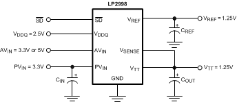 Figure 25. SSTL-2 Implementation with Higher Voltage Rails
9.2.4 Level Shifting
If standards other than SSTL-2 are required, such as SSTL-3, it may be necessary to use a different scaling factor than 0.5 times VDDQ for regulating the output voltage. Several options are available to scale the output to any voltage required. One method is to level shift the output by using feedback resistors from VTT to the VSENSE pin. This has been illustrated in Figure 26 and Figure 27. Figure 26 shows how to use two resistors to level shift VTT above the internal reference voltage of VDDQ/2. To calculate the exact voltage at VTT the following equation can be used.
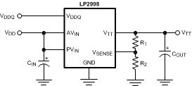 Figure 26. Increasing VTT by Level Shifting
Conversely, the R2 resistor can be placed between VSENSE and VDDQ to shift the VTT output lower than the internal reference voltage of VDDQ/2. The equations relating VTT and the resistors can be seen below:
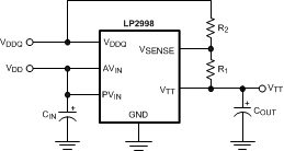 Figure 27. Decreasing VTT by Level Shifting
9.2.4.1 Output Capacitor Selection
For applications utilizing the LP2998 to terminate SSTL-2 I/O signals the typical application circuit shown in Figure 28 can be implemented.
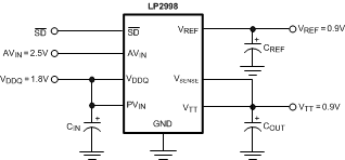 Figure 28. Typical SSTL-2 Application Circuit
This circuit permits termination in a minimum amount of board space and component count. Capacitor selection can be varied depending on the number of lines terminated and the maximum load transient. However, with motherboards and other applications where VTT is distributed across a long plane it is advisable to use multiple bulk capacitors and addition to high frequency decoupling. Figure 29 shown below depicts an example circuit where 2 bulk output capacitors could be situated at both ends of the VTT plane for optimal placement. Large aluminum electrolytic capacitors are used for their low ESR and low cost.
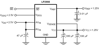 Figure 29. Typical SSTL-2 Application Circuit for Motherboards
In most PC applications an extensive amount of decoupling is required because of the long interconnects encountered with the DDR-SDRAM DIMMs mounted on modules. As a result bulk aluminum electrolytic capacitors in the range of 1000 µF are typically used.
9.2.5 HSTL Applications
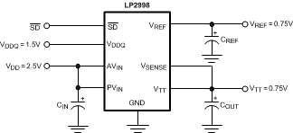
The LP2998 can be easily adapted for HSTL applications by connecting VDDQ to the 1.5 V rail. This will produce a VTT and VREF voltage of approximately 0.75 V for the termination resistors. AVIN and PVIN should be connected to a 2.5 V rail for optimal performance.
Figure 30. HSTL Application
9.2.6 QDR Applications
Quad data rate (QDR) applications utilize multiple channels for improved memory performance. However, this increase in bus lines has the effect of increasing the current levels required for termination. The recommended approach in terminating multiple channels is to use a dedicated LP2998 for each channel. This simplifies layout and reduces the internal power dissipation for each regulator. Separate VREF signals can be used for each DIMM bank from the corresponding regulator with the chipset reference provided by a local resistor divider or one of the LP2998 signals. Because VREF and VTT are expected to track and the part to part variations are minor, there should be little difference between the reference signals of each LP2998.
