SNAU266A July 2021 – August 2022
1 Abstract
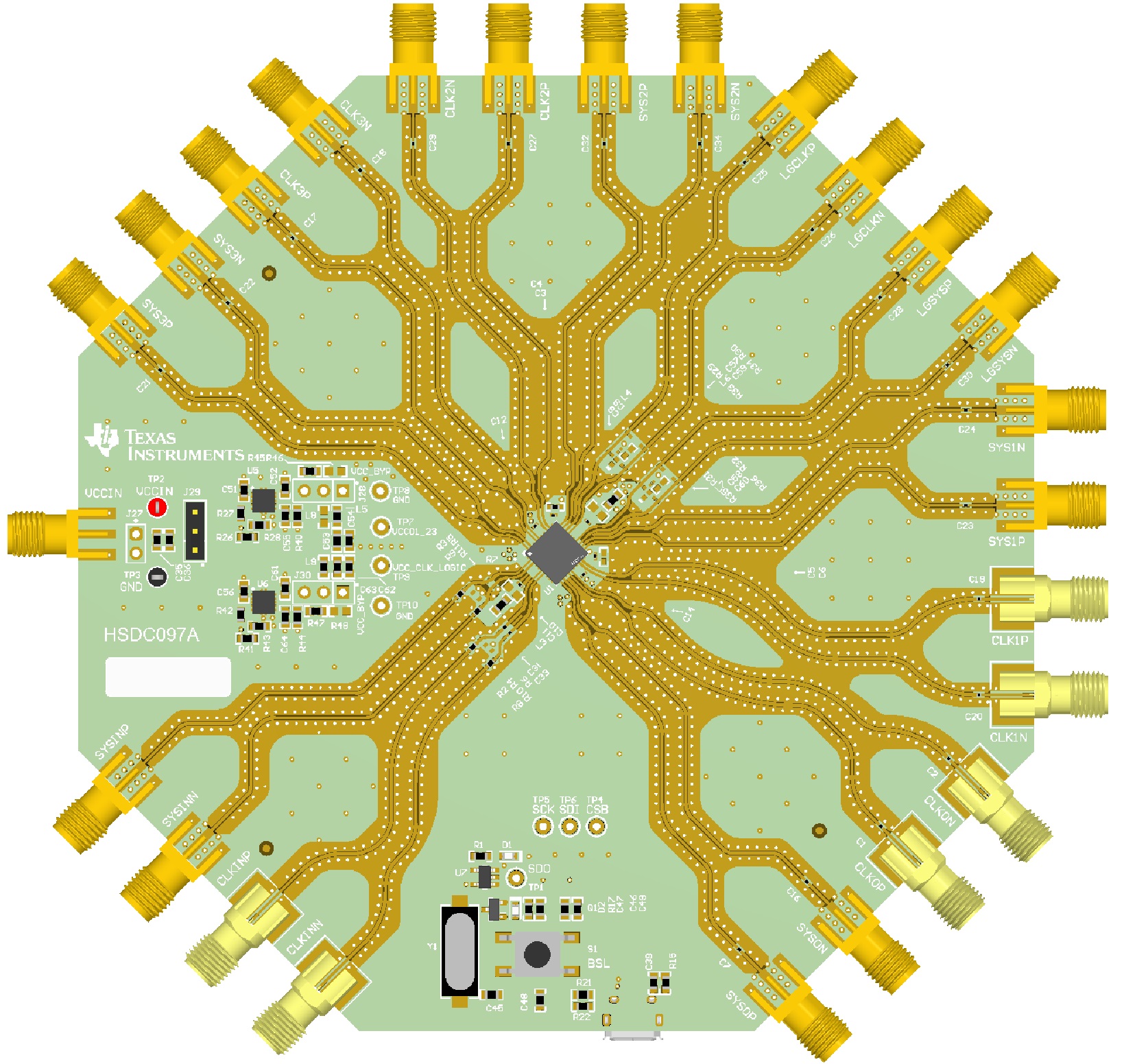
The LMX1204EVM is designed to evaluate the performance of LMX1204. This board consists of an LMX1204 device and an integrated USB2ANY programmer.
The LMX1204 is an ultra-low additive-jitter RF buffer, divider, and multiplier, with integrated SYSREF generation capability. The device can buffer RF frequencies up to 12.8 GHz, multiply RF outputs up to 6.4 GHz, and divide outputs by up to 8 GHz. A separate auxiliary clock divider can be used for FPGAs or other logic ICs. Each RF output (and the logic clock) is paired with a complementary SYSREF output with picosecond-precision delay-tuning capability, and can be operated as a generator (with synchronization capability across multiple devices) or as a repeater. The device runs from a single 2.5-V supply, and is programmed by a digital SPI interface from a 1.8-V, 2.5-V, or 3.3-V bus controller.