Data Sheet
TPS7H2211-SP 和 TPS7H2211-SEP 耐辐射保障 (RHA)
14V、3.5A 电子保险丝
本资源的原文使用英文撰写。 为方便起见,TI 提供了译文;由于翻译过程中可能使用了自动化工具,TI 不保证译文的准确性。 为确认准确性,请务必访问 ti.com 参考最新的英文版本(控制文档)。
1 特性
- 电离辐射总剂量 (TID) 特征值高达 100krad (Si)
- 提供的耐辐射保障为 100krad (Si)
- 确定了单粒子效应 (SEE)
- 单粒子锁定 (SEL)、单粒子烧毁 (SEB) 和单粒子栅穿 (SEGR) 对于线性能量传递 (LET) 的抗扰度高达 75MeV-cm2/mg*
- 单粒子功能中断 (SEFI) 和单粒子瞬变 (SET) 对于 LET 的额定抗扰度 = 75MeV-cm2/mg*
- 集成式单通道电子保险丝
- 输入电压范围:4.5V 至 14V
- 在 25°C 和 VIN = 12V 下的低导通电阻 (RON) 最大为 60mΩ
- 3.5A 最大连续开关电流
- 低控制输入阈值支持使用
1.2V、1.8V、2.5V 和 3.3V 逻辑电平 - 可配置上升时间(软启动)
- 反向电流保护 (RCP)
- 过压保护 (OVP)
- 内部电流限制(快速跳变)
- 热关断
- 带散热焊盘的陶瓷和塑料封装
- 支持军用(–55°C 至 125°C)温度范围
*请参阅 TPS7H2211-SP SEE 辐射报告,了解测试条件和完整信息
2 应用
- 卫星电力系统 (EPS)
- 冷备用电源(冗余)
- 电源时序
- 命令和数据处理
- 通信负载
- 耐辐射电源树
3 说明
TPS7H2211 是一款单通道电子保险丝(具有附加功能的集成 FET 负载开关),可提供反向电流保护、过压保护和可配置的上升时间,以便更大限度减少浪涌电流(软启动)。此器件包含一个可在 4.5V 至 14V 输入电压范围内运行的 P 沟道 MOSFET,并且支持最大 3.5A 的持续电流。
开关由可与低压控制信号直接连接的打开和关闭输入 (EN) 控制。过压保护和软启动可通过 OVP 和 SS 引脚使用很少的外部组件进行编程。TPS7H2211 采用具有外露散热焊盘的陶瓷和塑料封装,可提高散热性能。QML 5962R1822001VXC 提供了标准微电路图 (SMD)。-SEP 型号 V62/23609 提供了供应商项目图 (VID)。
器件信息
| 器件型号(1) | 等级(2) | 封装 |
|---|---|---|
| 5962R1822001VXC | 飞行等级 QMLV-RHA 100krad (Si) | 16 引脚 CFP 11.00mm × 9.60mm 质量 = 1.56g(4) |
| 5962-1822001VXC | 飞行等级 QMLV | |
| TPS7H2211HKR/EM | 工程样片(3) | |
| TPS7H2211MDAPTSEP | 9 月 | 32 引脚 HTSSOP 6.10mm × 11.00mm 质量 = 0.184g(4) |
| TPS7H2211EVM-CVAL | 评估模块 | 评估板 |
(1) 如需了解所有可用封装,请参阅数据表末尾的可订购产品附录。另请参阅器件选项表。
(2) 有关器件等级的其他信息,请查看 SLYB235。
(3) 这些器件仅适用于工程评估。器件按照不合规的流程进行加工处理。这些器件不适用于鉴定、量产、辐射测试或飞行。也不保证这些器件在 MIL 规定的 –55°C 至 125°C 完整温度范围内或运行寿命中的性能。
(4) 质量误差在 ±10% 以内。
 简化原理图
简化原理图4 Device Options
| GENERIC PART NUMBER | RADIATION RATING(1) | GRADE(2) | PACKAGE | ORDERABLE PART NUMBER |
|---|---|---|---|---|
| TPS7H2211-SP | TID of 100 krad(Si) RLAT, DSEE free to 75 MeV-cm2/mg |
QMLV-RHA | 16-pin HKR CFP | 5962R1822001VXC |
| QMLP-RHA | 32-pin DAP HTSSOP | 5962R1822002PYE | ||
| QMLV | 16-pin HKR CFP | 962-1822001VXC | ||
| KGD (QMLV-RHA) | Die | 5962R1822001V9A | ||
| None | Engineering model (3) | 16-pin HKR CFP | TPS7H2211HKR/EM | |
| Die | TPS7H2211Y/EM | |||
| TPS7H2211-SEP | TID of 50 krad(Si) RLAT, DSEE free to 43 MeV-cm2/mg |
Space Enhanced Plastic | 32-pin DAP HTSSOP | TPS7H2211MDAPTSEP |
(1) TID is total ionizing dose and
DSEE is destructive single event effects. Additional information is available in
the associated TID reports and SEE reports for each product.
(2) For additional information about
part grade, view SLYB235.
(3) These units are intended for
engineering evaluation only. They are processed to a non-compliant flow (such as
no burn-in and only 25°C testing). These units are not suitable for
qualification, production, radiation testing, or flight use. Parts are not
warranted as to performance over temperature or operating life.
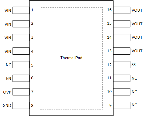
6 Pin Configuration and Functions
| HKR Package | DAP Package |
| 16-Pin CFP With Thermal Pad | 32-Pin HTSSOP With Thermal Pad |
| Top View | Top View |
 |
 |
Table 6-1 Pin Functions
| PIN | I/O(1) | DESCRIPTION | ||
|---|---|---|---|---|
| HKR (16) NO. | PW(32) NO. | NAME | ||
| 1-4 | 1-10 | VIN | I | Switch input. An input bypass capacitor is recommended for minimizing VIN dip. |
| 6 | 12 | EN | I | Active high switch control input. Do not float this pin. |
| 7 | 13 | OVP | I | Overvoltage protection. Set using an external resistor divider. If no OVP is desired, connect this pin to GND. Do not float this pin. |
| 8 | 15 | GND | — | Device ground. (2) |
| 12 | 22 | SS | I/O | Soft start (switch slew rate control). If this functionality is not desired, the SS pin must be left disconnected (floating). In all cases be sure to follow the requirements of Section 9.3.3. |
| 13-16 | 23-32 | VOUT | O | Switch output. A minimum 10-µF output capacitor is recommended. |
| 5, 9-11 | 11,14,16,17-21 | NC | — | NC — No connect. These pins are not internally connected. It is recommended to connect these pins to GND to prevent charge buildup; however, these pins can also be left open or tied to any voltage between GND and VIN. |
| — | Thermal Pad | — | Thermal pad (exposed center pad) for heat dissipation purposes. The thermal pad is internally connected to the seal ring and GND. | |
| — | Metal Lid | — | The lid is internally connected to the thermal pad and GND through the seal ring. | |
- I = Input, O = Output, I/O = Input or Output, — = Other
- Thermal pad is internally connected to the seal ring and GND for HKR option.
Table 6-2 Bare Die Information
| DIE THICKNESS | BACKSIDE FINISH | BACKSIDE POTENTIAL | BOND PAD METALLIZATION COMPOSITION | BOND PAD THICKNESS |
|---|---|---|---|---|
| 15 mils | Silicon with backgrind | Ground | AlCu | 1050 nm |

- All dimensions in microns (μm).
- The inner rectangle is the die and the outer rectangle is the die plus scribe lines.
Table 6-3 Bond Pad Coordinates in
Microns (μm)
| DESCRIPTION | PAD NUMBER | X MIN | Y MIN | X MAX | Y MAX |
|---|---|---|---|---|---|
| VIN | 1 | 653.22 | 4936.95 | 793.17 | 5076.9 |
| VIN | 2 | 152.37 | 4936.95 | 292.32 | 5076.9 |
| VIN | 3 | 319.32 | 4936.95 | 459.27 | 5076.9 |
| VIN | 4 | 486.27 | 4936.95 | 626.22 | 5076.9 |
| VIN | 5 | 152.37 | 4770 | 292.32 | 4909.95 |
| VIN | 6 | 319.32 | 4770 | 459.27 | 4909.95 |
| VIN | 7 | 486.27 | 4770 | 626.22 | 4909.95 |
| VIN | 8 | 653.22 | 4770 | 793.17 | 4909.95 |
| VIN | 9 | 152.37 | 4579.16 | 292.32 | 4719.11 |
| VIN | 10 | 319.32 | 4579.16 | 459.27 | 4719.11 |
| VIN | 11 | 486.27 | 4579.16 | 626.22 | 4719.11 |
| VIN | 12 | 653.22 | 4579.16 | 793.17 | 4719.11 |
| VIN | 13 | 152.37 | 4412.21 | 292.32 | 4552.16 |
| VIN | 14 | 319.32 | 4412.21 | 459.27 | 4552.16 |
| VIN | 15 | 486.27 | 4412.21 | 626.22 | 4552.16 |
| VIN | 16 | 653.22 | 4412.21 | 793.17 | 4552.16 |
| VIN | 17 | 152.37 | 3553.11 | 292.32 | 3693.06 |
| VIN | 18 | 319.32 | 3553.11 | 459.27 | 3693.06 |
| VIN | 19 | 486.27 | 3553.11 | 626.22 | 3693.06 |
| VIN | 20 | 653.22 | 3553.11 | 793.17 | 3693.06 |
| VIN | 21 | 152.37 | 3386.16 | 292.32 | 3526.11 |
| VIN | 22 | 319.32 | 3386.16 | 459.27 | 3526.11 |
| VIN | 23 | 486.27 | 3386.16 | 626.22 | 3526.11 |
| VIN | 24 | 653.22 | 3386.16 | 793.17 | 3526.11 |
| VINA(1) | 25 | 54.99 | 1823.09 | 194.94 | 1963.04 |
| VINA(1) | 26 | 54.99 | 1652.54 | 194.94 | 1792.49 |
| NC | 27 | 54.99 | 1480.77 | 194.94 | 1620.72 |
| NC | 28 | 54.99 | 1238.72 | 194.94 | 1378.67 |
| EN | 29 | 54.99 | 972.68 | 194.94 | 1112.63 |
| NC | 30 | 54.99 | 581.31 | 194.94 | 721.26 |
| OVP | 31 | 54.99 | 406.26 | 194.94 | 546.21 |
| GND | 32 | 407.21 | 54.99 | 547.16 | 194.94 |
| GND | 33 | 577.76 | 54.99 | 717.71 | 194.94 |
| NC | 34 | 2792.88 | 54.99 | 2932.83 | 194.94 |
| NC | 35 | 3315.06 | 587.43 | 3455.01 | 727.38 |
| NC | 36 | 3315.06 | 1099.26 | 3455.01 | 1239.21 |
| SS | 37 | 3315.06 | 1544.09 | 3455.01 | 1684.04 |
| VOUT | 38 | 3217.64 | 3386.16 | 3357.59 | 3526.11 |
| VOUT | 39 | 3050.69 | 3386.16 | 3190.64 | 3526.11 |
| VOUT | 40 | 2883.74 | 3386.16 | 3023.69 | 3526.11 |
| VOUT | 41 | 2716.79 | 3386.16 | 2856.74 | 3526.11 |
| VOUT | 42 | 3217.64 | 3553.11 | 3357.59 | 3693.06 |
| VOUT | 43 | 3050.69 | 3553.11 | 3190.64 | 3693.06 |
| VOUT | 44 | 2883.74 | 3553.11 | 3023.69 | 3693.06 |
| VOUT | 45 | 2716.79 | 3553.11 | 2856.74 | 3693.06 |
| VOUT | 46 | 3217.64 | 4412.21 | 3357.59 | 4552.16 |
| VOUT | 47 | 3050.69 | 4412.21 | 3190.64 | 4552.16 |
| VOUT | 48 | 2883.74 | 4412.21 | 3023.69 | 4552.16 |
| VOUT | 49 | 2716.79 | 4412.21 | 2856.74 | 4552.16 |
| VOUT | 50 | 3217.64 | 4579.16 | 3357.59 | 4719.11 |
| VOUT | 51 | 3050.69 | 4579.16 | 3190.64 | 4719.11 |
| VOUT | 52 | 2883.74 | 4579.16 | 3023.69 | 4719.11 |
| VOUT | 53 | 2716.79 | 4579.16 | 2856.74 | 4719.11 |
| VOUT | 54 | 3217.64 | 4770 | 3357.59 | 4909.95 |
| VOUT | 55 | 3050.69 | 4770 | 3190.64 | 4909.95 |
| VOUT | 56 | 2883.74 | 4770 | 3023.69 | 4909.95 |
| VOUT | 57 | 2716.79 | 4770 | 2856.74 | 4909.95 |
| VOUT | 58 | 3217.64 | 4936.95 | 3357.59 | 5076.9 |
| VOUT | 59 | 3050.69 | 4936.95 | 3190.64 | 5076.9 |
| VOUT | 60 | 2883.74 | 4936.95 | 3023.69 | 5076.9 |
| VOUT | 61 | 2716.79 | 4936.95 | 2856.74 | 5076.9 |
(1) VINA supplies internal circuitry.
Connect VINA to VIN in a single point manner.
7 Specifications
7.1 Absolute Maximum Ratings
over operating free-air temperature range (unless otherwise noted); all voltages referenced to GND(1)
| MIN | MAX | UNIT | |||
|---|---|---|---|---|---|
| VIN | Input voltage pins | –0.5 | 16 | V | |
| VOUT | Output voltage pins | –0.5 | 16 | V | |
| SS | Soft start pin | –0.3 | 16 | V | |
| EN, OVP | Enable and over voltage protection pins | –0.3 | 7.5 | V | |
| IIN, IOUT | Continuous switch current | 5.4 | A | ||
| IIN_PLS, IOUT_PLS | Pulsed switch current (t ≤ 5 µs) | 30 | A | ||
| TJ | Junction temperature | –55 | 150 | °C | |
| Tstg | Storage temperature | –65 | 150 | °C | |
(1) Operation outside the Absolute Maximum Ratings may cause permanent device damage. Absolute Maximum Ratings do not imply functional operation of the device at these or any other conditions beyond those listed under Recommended Operating Conditions. If used outside the Recommended Operating Conditions but within the Absolute Maximum Ratings, the device may not be fully functional, and this may affect device reliability, functionality, performance, and shorten the device lifetime.
7.2 ESD Ratings
| VALUE | UNIT | |||
|---|---|---|---|---|
| V(ESD) | Electrostatic discharge | Human-body model (HBM), per ANSI/ESDA/JEDEC JS-001(1) | ±2000 | V |
| Charged-device model (CDM), per ANSI/ESDA/JEDEC specification JS-002(2) | ±500 | |||
(1) JEDEC document JEP155 states that 500-V HBM allows safe manufacturing with a standard ESD control process. Manufacturing with less than 500-V HBM is possible with the necessary precautions.
(2) JEDEC document JEP157 states that 250-V CDM allows safe manufacturing with a standard ESD control process. Manufacturing with less than 250-V CDM is possible with the necessary precautions.
7.3 Recommended Operating Conditions
over operating free-air temperature range (unless otherwise noted); all voltages referenced to GND
| MIN | MAX | UNIT | |||
|---|---|---|---|---|---|
| VIN | Input voltage pins | 4.5 | 14 | V | |
| VOUT | Output voltage pins | 0 | 14(1) | V | |
| EN, OVP | Enable and overvoltage pins | 0 | 7 | V | |
| VINSR | Input voltage slew rate | 0.015 | V/µs | ||
| IIN, IOUT | Continuous switch current | 3.5 | A | ||
| TJ | Operating junction temperature(2) | –55 | 125 | °C | |
(1) This maximum VOUT voltage is only applicable when the device is disabled (EN = Low). When the device is enabled (EN = High), the maximum VOUT voltage is the input voltage, VIN.
(2) In applications where high power dissipation and/or poor package thermal resistance is present, the maximum ambient temperature may have to be derated. Maximum ambient temperature [TA(max)] is dependent on the maximum operating junction temperature [TJ(max)], the maximum power dissipation of the device in the application [PD(max)], and the junction-to-ambient thermal resistance of the part/package in the application (θJA), as given by the equation: TA(max) = TJ(max) – (θJA × PD(max))
7.4 Thermal Information
| THERMAL METRIC(1) | TPS7H2211-SP | TPS7H2211-SEP | UNIT | |
|---|---|---|---|---|
| HKR (CFP) | DAP (HTSSOP) | |||
| 16 PINS | 32 PINS | |||
| RθJA | Junction-to-ambient thermal resistance | 23 | 23.5 | °C/W |
| RθJC(top) | Junction-to-case (top) thermal resistance | 5.4 | 11.2 | |
| RθJB | Junction-to-board thermal resistance | 7.7 | 5.4 | |
| ψθJT | Junction-to-top characterization parameter | 1.3 | 0.1 | |
| ψθJB | Junction-to-board characterization parameter | 7.4 | 5.4 | |
| RθJC(bot) | Junction-to-case (bottom) thermal resistance | 0.33 | 0.5 | |
(1) For more information about traditional and new thermal metrics, see the Semiconductor and IC Package Thermal Metrics application report.
7.5 Electrical Characteristics: All Devices
over operating ambient temperature range TA = –55°C to 125°C, VIN = 4.5 to 14 V, COUT = 10 µF, and all voltages referenced to GND (unless otherwise noted); includes group E radiation testing at TA = 25°C for RHA devices(1)
| PARAMETER | TEST CONDITIONS | SUB- GROUP(2) |
MIN | TYP | MAX | UNIT | |||
|---|---|---|---|---|---|---|---|---|---|
| POWER SUPPLIES AND CURRENTS | |||||||||
| VINUVLOR | Internal VIN UVLO rising | 1, 2, 3 | 3.2 | 3.4 | 3.8 | V | |||
| VINUVLOF | Internal VIN UVLO falling | 1, 2, 3 | 2.6 | 2.9 | 3.2 | V | |||
| HYSTVIN-UVLO | Internal VIN UVLO hysteresis | 1, 2, 3 | 0.55 | 0.75 | V | ||||
| IQ | Quiescent current | IOUT = 0 mA, EN = 7 V | 1, 2, 3 | 5 | 10 | mA | |||
| IF | VIN to VOUT forward leakage current | EN = 0 V, VOUT = 0 V, measured VOUT current | VIN = 14 V | 1, 2, 3 | 1 | 1.3 | mA | ||
| VIN = 12 V | 1, 2, 3 | 0.65 | 0.94 | ||||||
| VIN = 9 V | 1, 2, 3 | 0.15 | 0.49 | ||||||
| VIN = 4.5 V | 1, 2, 3 | 0.04 | 0.23 | ||||||
| ISD VIN | VIN off-state supply current | EN = 0 V, VOUT = 0 V, measured VIN current | VIN = 14 V | 1, 2, 3 | 6.9 | 10 | mA | ||
| VIN = 12 V | 1, 2, 3 | 5.9 | 9.5 | ||||||
| VIN = 9 V | 1, 2, 3 | 4.4 | 8 | ||||||
| VIN = 4.5 V | 1, 2, 3 | 3.7 | 7 | ||||||
| VRCP_ENTER | Reverse current protection enter voltage(3) | EN = 7 V, see Figure 8-1 | VIN = 4.5 V | 1 | 390 | mV | |||
| VIN = 14 V | 1 | 363 | |||||||
| VRCP_EXIT | Reverse current protection exit voltage(3) | EN = 7 V, see Figure 8-2 | VIN = 4.5 V | 1 | 264 | mV | |||
| VIN = 14 V | 1 | 249 | |||||||
| tRCP | Reverse current protection response time | EN = 7 V, see Figure 8-1 | VIN = 4.5 V | 9 | 208 | µs | |||
| VIN = 14 V | 9 | 247 | |||||||
| IRCP | Reverse current protection leakage current | EN = 0 V, VOUT = 0 to 14 V and VOUT > VIN | 1, 2, 3 | 44 | 250 | µA | |||
| EN = 7 V, VIN = 0 V, VOUT = 0 to 14 V | 1, 2, 3 | 37 | 240 | ||||||
| SOFT START | |||||||||
| ISS | Soft start charge current | 1, 2, 3 | 65 | 83 | µA | ||||
| ENABLE (EN) INPUT | |||||||||
| VINEN | VIN percentage for enable (4) | 1, 2, 3 | 75% | ||||||
| IEN | EN pin input leakage current | EN = 7 V, VIN = 14 V | 1, 2, 3 | 2 | 12 | nA | |||
| OVERVOLTAGE PROTECTION (OVP) | |||||||||
| IOVP | OVP pin input leakage current | OVP = 7 V | 1, 2, 3 | 1.5 | 12 | nA | |||
| CURRENT LIMIT | |||||||||
| IL_trip | Internal current limit trip point | VIN = 12 V, CSS = 2 nF | 1 | 8 | A | ||||
| IL_peak | Fast trip off current limit peak | VIN = 12 V, 10 Ω to 10 mΩ short in 1 µs, switch inductance = 270 nH |
1 | 25 | A | ||||
| tftr | Fast trip off response time | 9 | 2.3 | µs | |||||
| tfto | Fast trip off off-time | VIN = 12 V, CSS = 2 nF | 9 | 51 | µs | ||||
| THERMAL SHUTDOWN | |||||||||
| Thermal shutdown | 155 | °C | |||||||
| Thermal shutdown hysteresis | 20 | °C | |||||||
(1) See the 5962-18220 SMD (standard microcircuit drawing) for additional information on the RHA devices.
(2) For subgroup definitions, see the Quality Conformance Inspection table
(3) This parameter is not referenced to GND; it is referenced from VOUT to VIN.
(4) VIN must be ≥ 75% of its final value before EN is asserted only if VINSR > VOUTSR.
7.6 Electrical Characteristics: CFP and KGD Options
over operating ambient temperature range TA = –55°C to 125°C, VIN = 4.5 to 14 V, COUT = 10 µF, and all voltages referenced to GND (unless otherwise noted); includes group E radiation testing at TA = 25°C for RHA devices(1)
| PARAMETER | TEST CONDITIONS | SUB- GROUP(2) |
MIN | TYP | MAX | UNIT | |||
|---|---|---|---|---|---|---|---|---|---|
| ENABLE (EN) INPUT | |||||||||
| VIHEN | EN threshold voltage, rising | 1, 2, 3 | 0.60 | 0.63 | 0.68 | V | |||
| VILEN | EN threshold voltage, falling | 1, 2, 3 | 0.50 | 0.52 | 0.57 | ||||
| HYSTEN | EN hysteresis voltage | 1, 2, 3 | 94 | 109 | 139 | mV | |||
| tLOW_OFF | EN signal low time during cycling | VOUT falls to < 90%, see RTIMER = 0 V, see Figure 8-3 | 9, 10, 11 | 20 | µs | ||||
| OVERVOLTAGE PROTECTION (OVP) | |||||||||
| VOVPR | OVP threshold voltage, rising | 1, 2, 3 | 1.11 | 1.15 | 1.18 | V | |||
| VOVPF | OVP threshold voltage, falling | 1, 2, 3 | 1.09 | 1.14 | 1.17 | ||||
| HYSTOVP | OVP hysteresis voltage | 4.6 V < VIN < 14 V | 1, 2, 3 | 5 | 14 | 40 | mV | ||
| RESISTANCE CHARACTERISTICS | |||||||||
| RON | On-state resistance, lead length ≈ 2.5 mm |
VIN = 14 V, IOUT = 3.5 A | –55°C | 3 | 41 | 45 | mΩ | ||
| –40°C | 43 | 46 | |||||||
| 25°C | 1 | 54 | 60 | ||||||
| 85°C | 65 | 71 | |||||||
| 125°C | 2 | 72 | 79 | ||||||
| VIN = 12 V, IOUT = 3.5 A | –55°C | 3 | 41 | 45 | |||||
| –40°C | 43 | 46 | |||||||
| 25°C | 1 | 54 | 60 | ||||||
| 85°C | 65 | 71 | |||||||
| 125°C | 2 | 72 | 79 | ||||||
| VIN = 9 V, IOUT = 3.5 A | –55°C | 3 | 41 | 45 | |||||
| –40°C | 43 | 46 | |||||||
| 25°C | 1 | 54 | 61 | ||||||
| 85°C | 65 | 71 | |||||||
| 125°C | 2 | 72 | 79 | ||||||
| VIN = 6 V, IOUT = 3.5 A | –55°C | 3 | 41 | 45 | |||||
| –40°C | 43 | 47 | |||||||
| 25°C | 1 | 54 | 61 | ||||||
| 85°C | 65 | 71 | |||||||
| 125°C | 2 | 72 | 79 | ||||||
| VIN = 4.5 V, IOUT = 3.5 A | –55°C | 3 | 44 | 48 | |||||
| –40°C | 47 | 50 | |||||||
| 25°C | 1 | 59 | 65 | ||||||
| 85°C | 71 | 76 | |||||||
| 125°C | 2 | 79 | 84 | ||||||
(1) See the 5962-18220 SMD (standard microcircuit drawing) for additional information on the RHA devices.
(2) For subgroup definitions, see the Quality Conformance Inspection table
7.7 Electrical Characteristics: HTSSOP Option
over operating ambient temperature range TA = –55°C to 125°C, VIN = 4.5 to 14 V, COUT = 10 µF, and all voltages referenced to GND (unless otherwise noted); includes group E radiation testing at TA = 25°C for RHA devices(1)
| PARAMETER | TEST CONDITIONS | SUB- GROUP(2) |
MIN | TYP | MAX | UNIT | |||
|---|---|---|---|---|---|---|---|---|---|
| ENABLE (EN) INPUT | |||||||||
| VIHEN | EN threshold voltage, rising | 1, 2, 3 | 0.59 | 0.63 | 0.67 | V | |||
| VILEN | EN threshold voltage, falling | 1, 2, 3 | 0.49 | 0.52 | 0.55 | ||||
| HYSTEN | EN hysteresis voltage | 1, 2, 3 | 95 | 106 | 116 | ||||
| tLOW_OFF | EN signal low time during cycling | VOUT falls to < 90%, see RTIMER = 0 V, see Figure 8-3 | 9, 10, 11 | 47 | µs | ||||
| OVERVOLTAGE PROTECTION (OVP) | |||||||||
| VOVPR | OVP threshold voltage, rising | 1, 2, 3 | 1.07 | 1.15 | 1.22 | V | |||
| VOVPF | OVP threshold voltage, falling | 1, 2, 3 | 1.04 | 1.12 | 1.19 | ||||
| HYSTOVP | OVP hysteresis voltage | 4.6 V < VIN < 14 V | 1, 2, 3 | 24 | 28 | 33 | mV | ||
| RESISTANCE CHARACTERISTICS | |||||||||
| RON | On-state resistance, lead length ≈ 2.5 mm |
VIN = 14 V, IOUT = 3.5 A | –55°C | 3 | 35.6 | 37 | mΩ | ||
| –40°C | 37.5 | ||||||||
| 25°C | 1 | 44.3 | 46 | ||||||
| 85°C | 53.7 | ||||||||
| 125°C | 2 | 56.3 | 60 | ||||||
| VIN = 12 V, IOUT = 3.5 A | –55°C | 3 | 35.3 | 37 | |||||
| –40°C | 37.3 | ||||||||
| 25°C | 1 | 44 | 46 | ||||||
| 85°C | 53.4 | ||||||||
| 125°C | 2 | 56 | 59 | ||||||
| VIN = 9 V, IOUT = 3.5 A | –55°C | 3 | 35 | 36 | |||||
| –40°C | 37 | ||||||||
| 25°C | 1 | 43.6 | 45 | ||||||
| 85°C | 53 | ||||||||
| 125°C | 2 | 55 | 58 | ||||||
| VIN = 6 V, IOUT = 3.5 A | –55°C | 3 | 34.8 | 36 | |||||
| –40°C | 37 | ||||||||
| 25°C | 1 | 43.5 | 45 | ||||||
| 85°C | 53 | ||||||||
| 125°C | 2 | 55.3 | 58 | ||||||
| VIN = 4.5 V, IOUT = 3.5 A | –55°C | 3 | 37.7 | 39 | |||||
| –40°C | 40 | ||||||||
| 25°C | 1 | 47.6 | 49 | ||||||
| 85°C | 58 | ||||||||
| 125°C | 2 | 61 | 63 | ||||||
(1) See the 5962-18220 SMD (standard microcircuit drawing) for additional information on the RHA devices.
(2) For subgroup definitions, see the Quality Conformance Inspection table
7.8 Switching Characteristics: All Devices
over operating ambient temperature TA = 25°C, COUT = 10 µF, CSS = 2 nF, RLOAD = 10 Ω (unless otherwise noted); all voltages referenced to GND
| PARAMETER | TEST CONDITIONS | SUBGROUP(1) | MIN | TYP | MAX | UNIT | |
|---|---|---|---|---|---|---|---|
| VIN = 5 V | |||||||
| tON | Turn-on time | See Figure 8-4 | 9 | 107 | µs | ||
| tOFF | Turn-off time | 56 | µs | ||||
| tF | VOUT fall time | 167 | µs | ||||
| tASSERT | OVP assert time | See Figure 8-5 | 9 | 8 | µs | ||
| tDEASSERT | OVP deassert time | 41 | µs | ||||
| VIN = 12 V | |||||||
| tON | Turn-on time | See Figure 8-4 | 9 | 220 | µs | ||
| tOFF | Turn-off time | 41 | µs | ||||
| tF | VOUT fall time | 139 | µs | ||||
| tASSERT | OVP assert time | See Figure 8-5 | 9 | 6 | µs | ||
| tDEASSERT | OVP deassert time | 63 | µs | ||||
(1) For subgroup definitions, see the Quality Conformance Inspection table
7.9 Quality Conformance Inspection
MIL-STD-883, Method 5005 - Group A
| SUBGROUP | DESCRIPTION | TEMPERATURE (°C) |
|---|---|---|
| 1 | Static tests at | 25 |
| 2 | Static tests at | 125 |
| 3 | Static tests at | –55 |
| 4 | Dynamic tests at | 25 |
| 5 | Dynamic tests at | 125 |
| 6 | Dynamic tests at | –55 |
| 7 | Functional tests at | 25 |
| 8A | Functional tests at | 125 |
| 8B | Functional tests at | –55 |
| 9 | Switching tests at | 25 |
| 10 | Switching tests at | 125 |
| 11 | Switching tests at | –55 |
7.10 Typical Characteristics
 Figure 7-1 IQ
vs Temperature Across VIN
Figure 7-1 IQ
vs Temperature Across VIN

| VIN = 0 V |

| No observed VIN dependency across measured values |

| No observed VIN dependency across measured values |


 Figure 7-2 IF
vs Temperature Across VIN
Figure 7-2 IF
vs Temperature Across VIN
| VIN = 0 V |


| No observed VIN dependency across measured values |

| No observed VIN dependency across measured values |


