ZHCSO27B May 2021 – December 2022 TPS7H4002-SP
PRODUCTION DATA
- 1 特性
- 2 应用
- 3 说明
- 4 Revision History
- 5 Pin Configuration and Functions
- 6 Specifications
-
7 Detailed Description
- 7.1 Overview
- 7.2 Functional Block Diagram
- 7.3
Feature Description
- 7.3.1 VIN and Power VIN Pins (VIN and PVIN)
- 7.3.2 Voltage Reference
- 7.3.3 Adjusting the Output Voltage
- 7.3.4 Safe Start-Up Into Prebiased Outputs
- 7.3.5 Error Amplifier
- 7.3.6 Slope Compensation
- 7.3.7 Enable and Adjust UVLO
- 7.3.8 Adjustable Switching Frequency and Synchronization (SYNC)
- 7.3.9 Slow Start (SS/TR)
- 7.3.10 Power Good (PWRGD)
- 7.3.11 Sequencing (SS/TR)
- 7.3.12 Output Overvoltage Protection (OVP)
- 7.3.13 Overcurrent Protection
- 7.3.14 Thermal Shutdown
- 7.3.15 Turn-On Behavior
- 7.3.16 Small Signal Model for Frequency Compensation
- 7.4 Device Functional Modes
-
8 Application and Implementation
- 8.1 Application Information
- 8.2
Typical Application
- 8.2.1 Design Requirements
- 8.2.2
Detailed Design Procedure
- 8.2.2.1 Operating Frequency
- 8.2.2.2 Output Inductor Selection
- 8.2.2.3 Output Capacitor Selection
- 8.2.2.4 Output Schottky Diode
- 8.2.2.5 Slow Start Capacitor Selection
- 8.2.2.6 Undervoltage Lockout (UVLO) Set Point
- 8.2.2.7 Output Voltage Feedback Resistor Selection
- 8.2.2.8 Compensation Component Selection
- 8.2.3 Parallel Operation
- 8.2.4 Application Curve
- 9 Power Supply Recommendations
- 10Layout
- 11Device and Documentation Support
- 12Mechanical, Packaging, and Orderable Information
8.2.2.8 Compensation Component Selection
There are several industry techniques used to compensate DC-DC regulators. For this design, type 2B compensation is used as shown in Small Signal Model for Frequency Compensation.
A good starting rule of thumb is to set the crossover frequency fco to roughly one-tenth of the converter switching frequency. This will generally provide good transient response and ensure that the modulator poles do not degrade phase margin. For this particular design, the target crossover frequency was set to be slightly lower than the rule of thumb at 30 kHz in order to optimize the phase margin of the frequency response.
The compensation components can be calculated using Equation 10 and Equation 11. The values calculated for R3 and C1 are 11.8 kΩ and 22 nF, respectively.
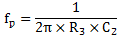
An additional high frequency pole can be used if necessary by adding a capacitor in parallel with the series combination of R3 and C1. The pole frequency is given by Equation 17.