ADC3660 16 位、0.5 至 65 MSPS、低噪声、低功率双通道 ADC
1 特性
- 双通道
- 16 位 65MSPS ADC(最大输出速率 = 31Msps)
- 本底噪声:-159dBFS/Hz
- 超低功耗:65MSPS 时为每通道 71mW
- 16 位,无丢码
- INL:±2LSB;DNL:±0.2LSB
- 基准:外部或内部
- 输入带宽:900MHz (3dB)
- 工业温度范围:-40°C 至 +105°C
- 片上数字下变频器
- 2 倍、4 倍、8 倍、16 倍、32 倍抽取率
- 32 位 NCO
- 串行 CMOS 接口
- 1.8V 单电源
- 小尺寸: 40 引脚 WQFN (5mm × 5mm) 封装
- 频谱性能 (fIN = 5MHz):
- SNR:81.9dBFS
- SFDR:88dBc HD2、HD3
- SFDR:102dBFS 最严重毛刺
3 说明
ADC3660 器件是一款低噪声、超低功耗、16 位、65MSPS 双通道高速模数转换器 (ADC)。该器件可实现低功耗,噪声频谱密度为 –159dBFS/Hz,还具有出色的线性度和动态范围。ADC3660 可实现出色的直流精度以及中频采样支持,因此是各种应用的出色选择。该 ADC 在 65MSPS 下的功耗仅为每通道 71mW,功耗随采样率减小而迅速降低。在旁路模式(最高 31MSPS)下,您可以在 1 或 2 个时钟周期后获取输出数据。
ADC3660 使用串行 CMOS (SCMOS) 接口输出数据,可更大限度减少数字互连的次数。该器件提供双通道、单通道和半通道选项。串行 CMOS 接口支持高达 250Mbps 的输出速率,相当于在复杂抽取后大约 15MSPS(双线)到大约 3.75MSPS(0.5 线)的输出速率。因此,ADC3660 可以使用内部抽取滤波器在“过采样和抽取”模式下运行,从而改进动态范围并省去外部抗混叠滤波器。
该器件采用 40 引脚 WQFN 封装(5mm × 5mm),支持 –40 至 +105⁰C 的工业级工作温度范围。
| 器件型号 (1) | 封装 | 封装尺寸(标称值) |
|---|---|---|
| ADC3660 | WQFN (40) | 5.00 × 5.00mm |
 FS = 65MSPS,Fin = 1MHz,16 倍抽取,实时
4 Revision History
Changes from Revision A (October 2020) to Revision B (March 2022)
- Changed the output clock jitter unit from ps to ps pk-pk in the Timing RequirementsGo
- Changed the ADC latency CMOS 2-wire NOM value from 1 to 2 and 1/2-wire NOM value from 2 to 1Go
- Changed Figure 8-3 Go
- Added GND symbol to REFGND pin for all voltage reference option diagramsGo
- Added the Output Bit Mapper sectionGo
- Added default power up configuration summary Table 8-11 Go
- Updated power-up initialization diagram Figure 9-4 with the correct indexing Go
5 Pin Configuration and Functions
") Figure 5-1 RSB Package, 40-Pin WQFN
Figure 5-1 RSB Package, 40-Pin WQFN(Top View)
| PIN | I/O | Description | |
|---|---|---|---|
| Name | No. | ||
| INPUT/REFERENCE | |||
| AINP | 12 | I | Positive analog input, channel A |
| AINM | 13 | I | Negative analog input, channel A |
| BINP | 39 | I | Positive analog input, channel B |
| BINM | 38 | I | Negative analog input, channel B |
| VCM | 8 | O | Common-mode voltage output for the analog inputs, 0.95 V |
| VREF | 2 | I | External voltage reference input, 1.6 V |
| REFBUF | 4 | I | 1.2V external voltage reference input for use with internal reference buffer. Internal 100 kΩ pull-up resistor to AVDD. This pin is also used to configure default operating conditions. |
| REFGND | 3 | I | Reference ground input, 0 V |
| CLOCK | |||
| CLKP | 6 | I | Positive differential sampling clock input for the ADC |
| CLKM | 7 | I | Negative differential sampling clock input for the ADC |
| CONFIGURATION | |||
| PDN/SYNC | 1 | I | Power down/Synchronization input. This pin can be configured via the SPI interface. Active high. This pin has an internal 21 kΩ pull-down resistor. |
| RESET | 9 | I | Hardware reset. Active high. This pin has an internal 21 kΩ pull-down resistor. |
| SEN | 16 | I | Serial interface enable. Active low. This pin has an internal 21 kΩ pull-up resistor to AVDD. |
| SCLK | 35 | I | Serial interface clock input. This pin has an internal 21 kΩ pull-down resistor. |
| SDIO | 10 | I/O | Serial interface data input and output. This pin has an internal 21 kΩ pull-down resistor. |
| NC | 17,19,20,22, 29,31,32,34 | - | Do not connect |
| DIGITAL INTERFACE | |||
| DA6 | 24 | O | CMOS data output. |
| DA5 | 23 | O | CMOS data output |
| FCLK | 18 | O | CMOS frame clock output |
| DB6 | 27 | O | CMOS data output. |
| DB5 | 28 | O | CMOS data output |
| DCLKIN | 33 | I | CMOS bit clock input |
| DCLK | 25 | O | CMOS bit clock output |
| POWER SUPPLY | |||
| AVDD | 5,15,36 | I | Analog 1.8V power supply |
| GND | 11,14,37,40, PowerPad | I | Ground, 0V |
| IOVDD | 21,30 | I | 1.8V power supply for digital interface |
| IOGND | 26 | I | Ground, 0V for digital interface |
6 Specifications
6.1 Absolute Maximum Ratings
| PARAMETER | TEST CONDITIONS | MIN | MAX | UNIT |
|---|---|---|---|---|
| Supply voltage range, AVDD, IOVDD | –0.3 | 2.1 | V | |
| Supply voltage range, GND, IOGND, REFGND | –0.3 | 0.3 | V | |
| Voltage applied to input pins | AINP/M, BINP/M, CLKP/M | –0.3 | 2.1 | V |
| VREF, REFBUF | –0.3 | 2.1 | ||
| PDN/SYNC, RESET, SCLK, SEN, SDIO, DCLKIN | –0.3 | 2.1 | ||
| Junction temperature, TJ | 105 | °C | ||
| Storage temperature, Tstg | –65 | 150 | °C | |
6.2 ESD Ratings
| VALUE | UNIT | |||
|---|---|---|---|---|
| V(ESD) | Electrostatic discharge | Human body model (HBM), per ANSI/ESDA/JEDEC JS-001, all pins(1) | 2500 | V |
| Charged device model (CDM), per JEDEC specification JESD22-C101, all pins(2) | 1000 | |||
6.3 Recommended Operating Conditions
| MIN | NOM | MAX | UNIT | |||
|---|---|---|---|---|---|---|
| Supply voltage range | AVDD(1) | 1.75 | 1.8 | 1.85 | V | |
| IOVDD(1) | 1.75 | 1.8 | 1.85 | V | ||
| TA | Operating free-air temperature | –40 | 105 | °C | ||
| TJ | Operating junction temperature | 105(2) | °C | |||
6.4 Thermal Information
| THERMAL METRIC(1) | ADC3660 | UNIT | |
|---|---|---|---|
| RSB (QFN) | |||
| 40 Pins | |||
| RΘJA | Junction-to-ambient thermal resistance | 30.7 | °C/W |
| RΘJC(top) | Junction-to-case (top) thermal resistance | 16.4 | °C/W |
| RΘJB | Junction-to-board thermal resistance | 10.5 | °C/W |
| ΨJT | Junction-to-top characterization parameter | 0.2 | °C/W |
| ΨJB | Junction-to-board characterization parameter | 10.5 | °C/W |
| RΘJC(bot) | Junction-to-case (bottom) thermal resistance | 2.0 | °C/W |
6.5 Electrical Characteristics - Power Consumption
| PARAMETER | TEST CONDITIONS | MIN | TYP | MAX | UNIT | |
|---|---|---|---|---|---|---|
| FS = 65 MSPS | ||||||
| IAVDD | Analog supply current | FS = 65 MSPS, External reference | 64 | 78 | mA | |
| IIOVDD | I/O supply current(1) | 8x real decimation, 2-wire CMOS | 15 | 20 | ||
| PDIS | Power dissipation(1) | External reference | 142 | 178 | mW | |
| IIOVDD | I/O supply current(1) | 16x real decimation, 1-wire CMOS | 14 | mA | ||
| 32x real decimation, 1-wire CMOS | 12 | mA | ||||
| 32x real decimation, 1/2-wire CMOS | 13 | mA | ||||
| 8x complex decimation, 2-wire CMOS | 19 | mA | ||||
| 16x complex decimation, 1-wire CMOS | 17 | mA | ||||
| 32x complex decimation, 1-wire CMOS | 15 | |||||
| 32x complex decimation, 1/2-wire CMOS | 16 | |||||
| MISCELLANEOUS | ||||||
| IAVDD | Internal reference, additional analog supply current | Enabled via SPI | 3 | mA | ||
| Internal reference buffer, additional analog supply current | 0.3 | |||||
| Single ended clock input, reduces analog supply current by | 0.7 | |||||
| PDIS | Power consumption in global power down mode | Default mask settings, internal reference | 5 | mW | ||
| Default mask settings, external reference | 9 | |||||
6.6 Electrical Characteristics - DC Specifications
| PARAMETER | TEST CONDITIONS | MIN | TYP | MAX | UNIT | |
|---|---|---|---|---|---|---|
| DC ACCURACY | ||||||
| No missing codes | 16 | bits | ||||
| PSRR | FIN = 1 MHz | 50 | dB | |||
| DNL | Differential nonlinearity | FIN = 5 MHz | -0.5 | ± 0.2 | +1 | LSB |
| INL(1) | Integral nonlinearity | FIN = 5 MHz | -4.5 | ± 2 | +4.5 | LSB |
| VOS_ERR | Offset error | -130 | 2 | 130 | LSB | |
| VOS_DRIFT | Offset drift over temperature | -3.5 | LSB/ºC | |||
| GAINERR | Gain error | External 1.6V Reference | 0 | %FSR | ||
| GAINDRIFT | Gain drift over temperature | External 1.6V Reference | 10.3 | ppm/ºC | ||
| GAINERR | Gain error | Internal Reference | 2.4 | %FSR | ||
| GAINDRIFT | Gain drift over temperature | Internal Reference | 108.8 | ppm/ºC | ||
| Transition Noise | 1.5 | LSB | ||||
| ADC ANALOG INPUT (AINP/M, BINP/M) | ||||||
| FS | Input full scale | Differential | 3.2 | Vpp | ||
| VCM | Input common model voltage | 0.9 | 0.95 | 1.0 | V | |
| RIN | Differential input resistance | FIN = 100 kHz | 8 | kΩ | ||
| CIN | Differential input Capacitance | FIN = 100 kHz | 7 | pF | ||
| VOCM | Output common mode voltage | 0.95 | V | |||
| BW | Analog Input Bandwidth (-3dB) | 900 | MHz | |||
| INTERNAL VOLTAGE REFERENCE | ||||||
| VREF | Internal reference voltage | 1.6 | V | |||
| VREF Output Impedance | 8 | Ω | ||||
| REFERENCE INPUT BUFFER (REFBUF) | ||||||
| External reference voltage | 1.2 | V | ||||
| EXTERNAL VOLTAGE REFERENCE (VREF) | ||||||
| VREF | External voltage reference | 1.6 | V | |||
| Input Current | 0.3 | mA | ||||
| Input impedance | 5.3 | kΩ | ||||
| CLOCK INPUT (CLKP/M) | ||||||
| Input clock frequency | 0.5 | 65 | MHz | |||
| VID | Differential input voltage | 1 | 3.6 | Vpp | ||
| VCM | Input common mode voltage | 0.9 | V | |||
| RIN | Single ended input resistance to common mode. | 5 | kΩ | |||
| CIN | Single ended input capacitance | 1.5 | pF | |||
| Clock duty cycle | 40 | 50 | 60 | % | ||
| DIGITAL INPUTS (RESET, PDN, SCLK, SEN, SDIO) | ||||||
| VIH | High level input voltage | 1.4 | V | |||
| VIL | Low level input voltage | 0.4 | V | |||
| IIH | High level input current | 90 | 150 | uA | ||
| IIL | Low level input current | -150 | -90 | uA | ||
| CI | Input capacitance | 1.5 | pF | |||
| DIGITAL OUTPUT (SDOUT) | ||||||
| VOH | High level output voltage | ILOAD = -400 uA | IOVDD – 0.1 | IOVDD | V | |
| VOL | Low level output voltage | ILOAD = 400 uA | 0.1 | V | ||
| DIGITAL SCMOS OUTPUTS (DA5/6, DB5/6) | ||||||
| Output data rate | per CMOS output pin | 250 | MHz | |||
| VOH | High level output voltage | IOVDD – 0.1 | IOVDD | V | ||
| VOL | Low level output voltage | ILOAD = 400 uA | 0.1 | V | ||
| VIH | High level input voltage | DCLKIN | IOVDD – 0.1 | IOVDD | V | |
| VIL | Low level input voltage | 0.1 | V | |||
6.7 Electrical Characteristics - AC Specifications
| PARAMETER | TEST CONDITIONS | MIN | TYP | MAX | UNIT | |
|---|---|---|---|---|---|---|
| NSD | Noise Spectral Density | fIN = 1.1 MHz, AIN = -20 dBFS | -159 | dBFS/Hz | ||
| SNR(1) | Signal to noise ratio | fIN = 1.1 MHz | 82.0 | dBFS | ||
| fIN = 5 MHz | 77.5 | 81.9 | ||||
| fIN = 10 MHz | 81.2 | |||||
| fIN = 20 MHz | 79.9 | |||||
| fIN = 40 MHz | 77.6 | |||||
| fIN = 64 MHz | 74.6 | |||||
| SNR | Signal to noise ratio, complex decimation by 16 | fIN = 1.1 MHz, fNCO = 2.5 MHz | 88.3 | dBFS | ||
| fIN = 5 MHz, fNCO = 5 MHz | 89.2 | |||||
| fIN = 10 MHz, fNCO = 10 MHz | 89.3 | |||||
| fIN = 20 MHz, fNCO = 20 MHz | 88.7 | |||||
| fIN = 40 MHz, fNCO = 40 MHz | 86.5 | |||||
| fIN = 64 MHz, fNCO = 62.6 MHz | 84.3 | |||||
| SINAD(1) | Signal to noise and distortion ratio | fIN = 1.1 MHz | 80.0 | dBFS | ||
| fIN = 5 MHz | 76.2 | 80.9 | ||||
| fIN = 10 MHz | 80.8 | |||||
| fIN = 20 MHz | 78.1 | |||||
| fIN = 40 MHz | 76.2 | |||||
| fIN = 64 MHz | 73.6 | |||||
| ENOB(1) | Effective number of bits | fIN = 1.1 MHz | 13.3 | bit | ||
| fIN = 5 MHz | 12.6 | 13.3 | ||||
| fIN = 10 MHz | 13.2 | |||||
| fIN = 20 MHz | 13.0 | |||||
| fIN = 40 MHz | 12.6 | |||||
| fIN = 64 MHz | 12.1 | |||||
| THD(1) | Total Harmonic Distortion (First five harmonics) | fIN = 1.1 MHz | 83 | dBc | ||
| fIN = 5 MHz | 81 | 87 | ||||
| fIN = 10 MHz | 90 | |||||
| fIN = 20 MHz | 82 | |||||
| fIN = 40 MHz | 81 | |||||
| fIN = 64 MHz | 80 | |||||
| SFDR(1) | Spur free dynamic range including second and third harmonic | fIN = 1.1 MHz | 84 | dBc | ||
| fIN = 5 MHz | 83 | 88 | ||||
| fIN = 10 MHz | 94 | |||||
| fIN = 20 MHz | 85 | |||||
| fIN = 40 MHz | 83 | |||||
| fIN = 64 MHz | 84 | dBc | ||||
| Non HD2,3(1) | Spur free dynamic range (excluding HD2 and HD3) | fIN = 1.1 MHz | 101 | dBFS | ||
| fIN = 5 MHz | 91 | 102 | ||||
| fIN = 10 MHz | 99 | |||||
| fIN = 20 MHz | 95 | |||||
| fIN = 40 MHz | 93 | |||||
| fIN = 64 MHz | 87 | |||||
| IMD3 | Two tone inter-modulation distortion | f1 = 3 MHz, f2 = 4 MHz, AIN = -7 dBFS/tone | 88 | dBc | ||
| f1 = 10 MHz, f2 = 12 MHz, AIN = -7 dBFS/tone | 90 | |||||
6.8 Timing Requirements
| PARAMETER | TEST CONDITIONS | MIN | NOM | MAX | UNIT | |
|---|---|---|---|---|---|---|
| ADC TIMING SPECIFICATIONS | ||||||
| tAD | Aperture Delay | 0.85 | ns | |||
| tA | Aperture Jitter | square wave clock with fast edges | 180 | fs | ||
| tJ | Jitter on DCLKIN | ± 50 | ps pk-pk | |||
| tACQ | Signal acquisition period, Default | referenced to sampling clock falling edge | -TS/4 | Sampling Clock Period | ||
| tCONV | Signal conversion period | referenced to sampling clock falling edge | 10 | ns | ||
| Wake up time | Time to valid data after coming out of power down. Internal reference. | Bandgap reference enabled, single ended clock | 14.6 | us | ||
| Bandgap reference enabled, differential clock | 14.0 | |||||
| Bandgap reference disabled, single ended clock | 1.7 | ms | ||||
| Bandgap reference disabled, differential clock | 2.1 | |||||
| Time to valid data after coming out of power down. External 1.6V reference. | Bandgap reference enabled, single ended clock | 14.6 | us | |||
| Bandgap reference enabled, differential clock | 14.0 | |||||
| Bandgap reference disabled, single ended clock | 1.8 | ms | ||||
| Bandgap reference disabled, differential clock | 1.7 | |||||
| tS,SYNC | Setup time for SYNC input signal | Referenced to sampling clock rising edge | 500 | ps | ||
| tH,SYNC | Hold time for SYNC input signal | 600 | ||||
| ADC Latency | Signal input to data output | Serialized CMOS: 2-wire | 2 | ADC clock cycles | ||
| Serialized CMOS: 1-wire | 1 | |||||
| Serialized CMOS: 1/2-wire | 1 | |||||
| Add. Latency | Real decimation by 2 | 21 | Output clock cycles | |||
| Complex decimation by 2 | 22 | |||||
| Real or complex decimation by 4, 8, 16, 32 | 23 | |||||
| INTERFACE TIMING | ||||||
| tPD | Propagation delay: sampling clock falling edge to DCLK rising edge | Delay between sampling clock falling edge to DCLKIN falling edge < 2.5ns. TDCLK = DCLK period tCDCLK = Sampling clock falling edge to DCLKIN falling edge |
2 + TDCLK + tCDCLK | 3 + TDCLK + tCDCLK | 4 + TDCLK + tCDCLK | ns |
| Delay between sampling clock falling edge to DCLKIN falling edge >= 2.5ns. TDCLK = DCLK period tCDCLK = Sampling clock falling edge to DCLKIN falling edge |
2 + tCDCLK | 3 + tCDCLK | 4 + tCDCLK | |||
| tCD | DCLK rising edge to output data delay 2-wire serial CMOS |
Fout = 10 MSPS, DA/B5,6 = 80 MBPS | -0.24 | 0.10 | ns | |
| Fout = 20 MSPS, DA/B5,6 = 160 MBPS | -0.29 | 0.10 | ||||
| Fout = 30 MSPS, DA/B5,6 = 240 MBPS | -0.28 | 0.09 | ||||
| DCLK rising edge to output data delay 1-wire serial CMOS |
Fout = 5 MSPS, DA/B6 = 80 MBPS | -0.22 | 0.11 | |||
| Fout = 10 MSPS, DA/B6 = 160 MBPS | -0.27 | 0.11 | ||||
| Fout = 15 MSPS, DA/B6 = 240 MBPS | -0.52 | 0.08 | ||||
| DCLK rising edge to output data delay 1/2-wire serial CMOS |
Fout = 5 MSPS, DA6 = 160 MBPS | -0.24 | 0.1 | |||
| tDV | Data valid, 2-wire serial CMOS | Fout = 10 MSPS, DA/B5,6 = 80 MBPS | 12.19 | 12.36 | ns | |
| Fout = 20 MSPS, DA/B5,6 = 160 MBPS | 5.93 | 6.1 | ||||
| Fout = 30 MSPS, DA/B5,6 = 240 MBPS | 3.91 | 4.07 | ||||
| Data valid, 1-wire serial CMOS | Fout = 5 MSPS, DA/B6 = 80 MBPS | 12.21 | 12.39 | |||
| Fout = 10 MSPS, DA/B6 = 160 MBPS | 5.95 | 6.10 | ||||
| Fout = 15 MSPS, DA/B6 = 240 MBPS | 3.83 | 4.08 | ||||
| Data valid, 1/2-wire serial CMOS | Fout = 5 MSPS, DA6 = 160 MBPS | 5.36 | 6.13 | |||
| SERIAL PROGRAMMING INTERFACE (SCLK, SEN, SDIO) - Input | ||||||
| fCLK,SCLK | Serial clock frequency | 20 | MHz | |||
| tS,SEN | SEN falling edge to SCLK rising edge | 10 | ns | |||
| tH,SEN | SCLK rising edge to SEN rising edge | 9 | ||||
| tS,SDIO | SDIO setup time from rising edge of SCLK | 17 | ||||
| tH,SDIO | SDIO hold time from rising edge of SCLK | 9 | ||||
| SERIAL PROGRAMMING INTERFACE (SDIO) - Output | ||||||
| tOZD | Delay from falling edge of 16th SCLK cycle during read operation for SDIO transition from tri-state to valid data | 3.9 | 10.8 | ns | ||
| tODZ | Delay from SEN rising edge for SDIO transition from valid data to tri-state | 3.4 | 14 | |||
| tOD | Delay from falling edge of 16th SCLK cycle during read operation to SDIO valid | 3.9 | 10.8 | |||
6.9 Typical Characteristics
Typical values at TA = 25 °C, ADC sampling rate = 65 MSPS, AIN = –1 dBFS differential input, 50% clock duty cycle, AVDD = IOVDD = 1.8 V, external 1.6 V reference, 5 pF output load, unless otherwise noted.


| Decimation by 32, complex. NCO = 10.1 MHz |


| FS = 25 MSPS, Decimation by 8, real |


| FIN = 5 MHz, 50 mVpp signal on AVDD |

| FIN = 1 MHz, 16-bit resolution, 2-w |


| Decimation by 16, real |


| Aggressor at -1 dBFS |

| FIN = 1 MHz, 32x complex decimation, 16-bit resolution |

| FIN = 1 MHz, 32x complex decimation, 16-bit resolution, 2-w |
Decimation bypass mode is for full Nyquist zone illustration only.
7 Parameter Measurement Information
") Figure 7-1 Timing diagram: 2-wire SCMOS (changed from 18-bit to 16-bit output after power up)
Figure 7-1 Timing diagram: 2-wire SCMOS (changed from 18-bit to 16-bit output after power up)") Figure 7-2 Timing diagram: 1-wire SCMOS (changed from 18-bit to 16-bit output after power up)
Figure 7-2 Timing diagram: 1-wire SCMOS (changed from 18-bit to 16-bit output after power up)") Figure 7-3 Timing diagram: 1/2-wire SCMOS (changed from 18-bit to 16-bit output after power up)
Figure 7-3 Timing diagram: 1/2-wire SCMOS (changed from 18-bit to 16-bit output after power up)8 Detailed Description
8.1 Overview
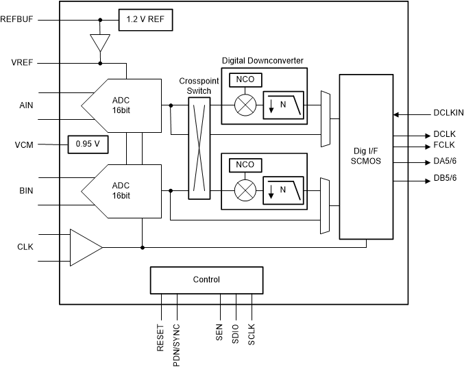
The ADC3660 is a low noise, ultra-low power 16-bit high-speed dual channel ADC family supporting sampling rates up to 65Msps. It offers excellent DC precision together with IF sampling support which makes it ideally suited for a wide range of applications. The ADC3660 is equipped with an internal reference option but it also supports the use of an external, high precision 1.6V voltage reference or an external 1.2V reference which is buffered and gained up internally.
An optional programmable digital down converter enables external anti-alias filter relaxation as well as output data rate reduction. The digital filter provides a 32-bit programmable NCO and supports both real or complex decimation.
- Decimation Bypass Mode: ~ 31 Msps (2-wire) to ~ 8 Msps (0.5-wire)
- Complex Decimation: ~ 15 Msps (2-wire) to ~4 Msps (0.5-wire)
- Real Decimation: ~ 30 Msps (2-wire) to ~ 8 Msps (0.5-wire)
The ADC3660 includes a digital output formatter which supports output resolutions from 14 to 20-bit.
The device features and control options can be set up either through pin configurations or via SPI register writes.
8.2 Functional Block Diagram
8.3 Feature Description
8.3.1 Analog Input
The analog inputs of ADC3660 are intended to be driven differentially. Both AC coupling and DC coupling of the analog inputs is supported. The analog inputs are designed for an input common mode voltage of 0.95 V which must be provided externally on each input pin. DC-coupled input signals must have a common mode voltage that meets the device input common mode voltage range.
The equivalent input network diagram is shown in Figure 8-1. All four sampling switches, on-resistance shown in red, are in same position (open or closed) simultaneously.
 Figure 8-1 Equivalent Input Network
8.3.1.1 Analog Input Bandwidth
Figure 8-2 shows the analog full power input bandwidth of the ADC3660 with a 50 Ω differential termination. The -3 dB bandwidth is approximately 900 MHz and the useful input bandwidth with good AC performance is approximately 120 MHz.
The equivalent differential input resistance RIN and input capacitance CIN vs frequency are shown in Figure 8-3.
 Figure 8-2 ADC Analog Input Bandwidth Response
8.3.1.2 Analog Front End Design
The ADC3660 is an unbuffered ADC and thus a passive kick-back filter is recommended to absorb the glitch from the sampling operation. Depending on if the input is driven by a balun or a differential amplifier with low output impedance, a termination network may be needed. Additionally a passive DC bias circuit is needed in AC-coupled applications which can be combined with the termination network.
8.3.1.2.1 Sampling Glitch Filter Design
The front end sampling glitch filter is designed to optimize the SNR and HD3 performance of the ADC. The filter performance is dependent on input frequency and therefore the following filter designs are recommended for different input frequency ranges as shown in Figure 8-4 and Figure 8-5 (assuming 50 Ω source impedance).
 Figure 8-4 Sampling
glitch filter for input frequencies from DC to 30 MHz
Figure 8-4 Sampling
glitch filter for input frequencies from DC to 30 MHz Figure 8-5 Sampling
glitch filter for input frequencies from 30 to 70 MHz
Figure 8-5 Sampling
glitch filter for input frequencies from 30 to 70 MHz8.3.1.2.2 Analog Input Termination and DC Bias
Depending on the input drive circuitry, a termination network and/or DC biasing needs to be provided.
8.3.1.2.2.1 AC-Coupling
The ADC3660 requires external DC bias using the common mode output voltage (VCM) of the ADC together with the termination network as shown in Figure 8-6. The termination is located within the glitch filter network. When using a balun on the input, the termination impedance has to be adjusted to account for the turns ratio of the transformer. When using an amplifier, the termination impedance can be adjusted to optimize the amplifier performance.
") Figure 8-6 AC-Coupling: termination network provides DC bias (glitch filter example for DC - 30 MHz)
Figure 8-6 AC-Coupling: termination network provides DC bias (glitch filter example for DC - 30 MHz)