ZHCSLC3B may   2020  – april 2023 TPD3S713-Q1 , TPD3S713A-Q1

PRODUCTION DATA  

  1.   1
  2. 特性
  3. 应用
  4. 说明
  5. Revision History
  6. Pin Configuration and Functions
  7. Specifications
    1. 6.1 Absolute Maximum Ratings
    2. 6.2 ESD Ratings
    3. 6.3 Recommended Operating Conditions
    4. 6.4 Thermal Information
    5. 6.5 Electrical Characteristics
    6. 6.6 Switching Characteristics
    7. 6.7 Typical Characteristics
  8. Parameter Measurement Information
  9. Detailed Description
    1. 8.1 Overview
    2. 8.2 Functional Block Diagram
    3. 8.3 Feature Description
      1. 8.3.1 FAULT Response
      2. 8.3.2 Cable Compensation
        1. 8.3.2.1 Design Procedure
      3. 8.3.3 DP and DM Protection
      4. 8.3.4 VBUS OVP Protection
      5. 8.3.5 Output and DP or DM Discharge
      6. 8.3.6 Overcurrent Protection
      7. 8.3.7 Undervoltage Lockout
      8. 8.3.8 Thermal Sensing
      9. 8.3.9 Current-Limit Setting
    4. 8.4 Device Functional Modes
      1. 8.4.1 Device Truth Table (TT)
      2. 8.4.2 Client Mode
      3. 8.4.3 High-Bandwidth Data-Line Switch
  10. Application and Implementation
    1. 9.1 Application Information
    2. 9.2 Typical Application
      1. 9.2.1 Design Requirements
      2. 9.2.2 Detailed Design Procedure
        1. 9.2.2.1 Input Capacitance
        2. 9.2.2.2 Output Capacitance
        3. 9.2.2.3 BIAS Capacitance
        4. 9.2.2.4 Output and BIAS TVS
      3. 9.2.3 Application Curves
    3. 9.3 Power Supply Recommendations
    4. 9.4 Layout
      1. 9.4.1 Layout Guidelines
      2. 9.4.2 Layout Example
  11. 10Device and Documentation Support
    1. 10.1 Documentation Support
      1. 10.1.1 Related Documentation
    2. 10.2 接收文档更新通知
    3. 10.3 支持资源
    4. 10.4 Trademarks
    5. 10.5 静电放电警告
    6. 10.6 术语表
  12. 11Mechanical, Packaging, and Orderable Information

Cable Compensation

When a load draws current through a long or thin wire, there is an IR drop that reduces the voltage delivered to the load. In the vehicle from the voltage regulator 5-V output to the loading, the total resistance of power switch rDS(on) and cable resistance causes an IR drop at the loading input. So the charging current of most portable devices is less than their expected maximum charging current.
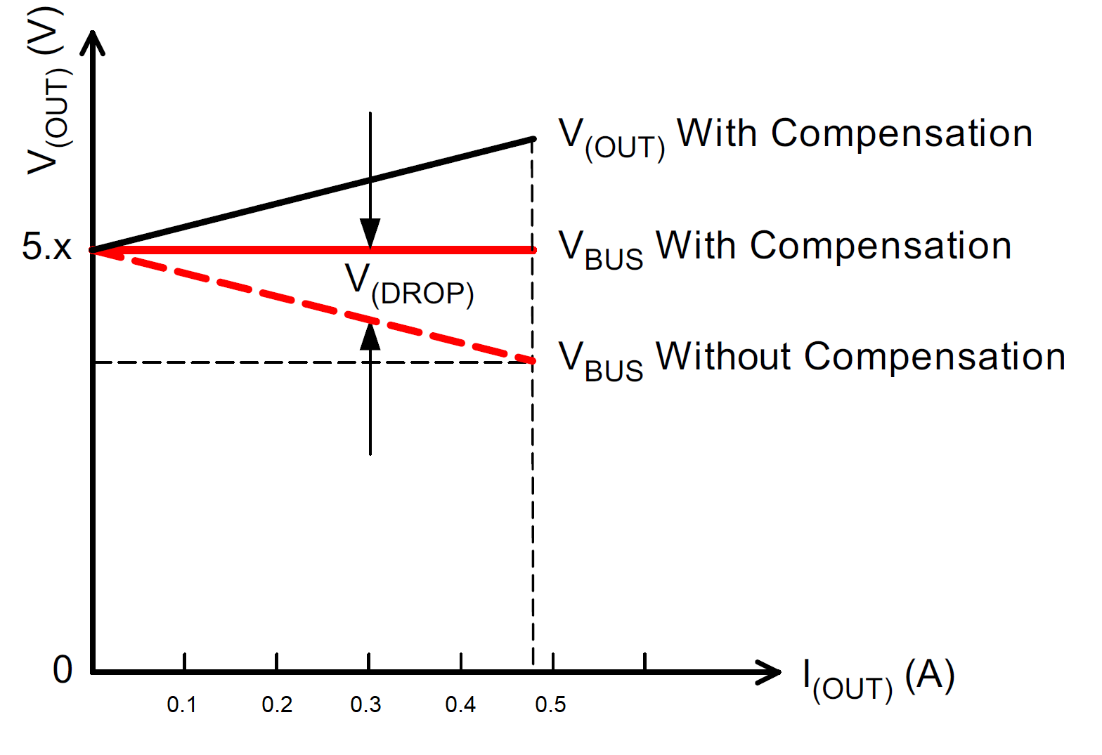
GUID-7097A96B-6889-41E8-AAB9-CC59DD926DBD-low.pngFigure 8-1 Voltage Drop

The TPD3S713-Q1 device detects the load current and applies a proportional sink current that can be used to adjust the output voltage of the upstream regulator to compensate for the IR drop in the charging path. The gain G(CS) of the sink current proportional to load current is 420 µA/A.
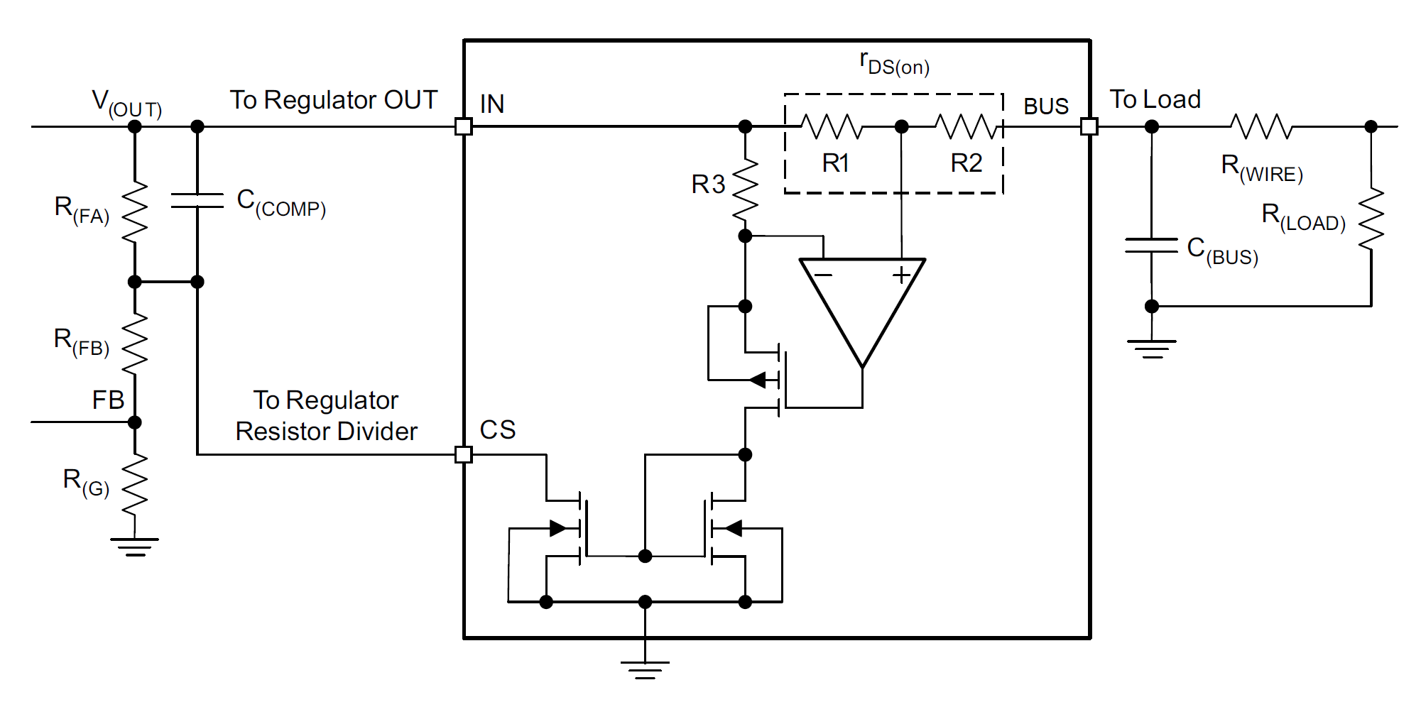
GUID-A1E8A197-61D4-425F-9986-BA534256289D-low.pngFigure 8-2 Cable Compensation Equivalent Circuit