ZHCSJH9A August   2019  – August 2019 TPS56C230

PRODUCTION DATA.  

  1. 1 特性
  2. 2 应用
  3. 3 说明
    1.     Device Images
      1.      简化原理图
      2.      效率与输出电流 Eco-mode
  4. 4 修订历史记录
  5. 5 Pin Configuration and Functions
    1.     Pin Functions
  6. 6 Specifications
    1. 6.1 Absolute Maximum Ratings
    2. 6.2 ESD Ratings
    3. 6.3 Recommended Operating Conditions
    4. 6.4 Thermal Information
    5. 6.5 Electrical Characteristics
    6. 6.6 Typical Characteristics
  7. 7 Detailed Description
    1. 7.1 Overview
    2. 7.2 Functional Block Diagram
    3. 7.3 Feature Description
      1. 7.3.1  PWM Operation and D-CAP3 Control
      2. 7.3.2  Soft Start
      3. 7.3.3  Large Duty Operation
      4. 7.3.4  Power Good
      5. 7.3.5  Overcurrent Protection and Undervoltage Protection
      6. 7.3.6  Overvoltage Protection
      7. 7.3.7  Out-of-Bounds Operation
      8. 7.3.8  UVLO Protection
      9. 7.3.9  Output Voltage Discharge
      10. 7.3.10 Thermal Shutdown
    4. 7.4 Device Functional Modes
      1. 7.4.1 Light Load Operation
      2. 7.4.2 Eco-mode Control
      3. 7.4.3 Force CCM
      4. 7.4.4 Mode Selection
      5. 7.4.5 Standby Operation
  8. 8 Application and Implementation
    1. 8.1 Application Information
    2. 8.2 Typical Application
      1. 8.2.1 Design Requirements
      2. 8.2.2 Detailed Design Procedure
        1. 8.2.2.1 Custom Design With WEBENCH® Tools
        2. 8.2.2.2 Output Voltage Set Point
        3. 8.2.2.3 MODE Selection
        4. 8.2.2.4 Inductor Selection
        5. 8.2.2.5 Output Capacitor Selection
        6. 8.2.2.6 Input Capacitor Selection
      3. 8.2.3 Application Curves
  9. 9 Power Supply Recommendations
  10. 10Layout
    1. 10.1 Layout Guidelines
    2. 10.2 Layout Example
  11. 11器件和文档支持
    1. 11.1 器件支持
      1. 11.1.1 第三方产品免责声明
      2. 11.1.2 开发支持
        1. 11.1.2.1 使用 WEBENCH® 工具创建定制设计
    2. 11.2 接收文档更新通知
    3. 11.3 社区资源
    4. 11.4 商标
    5. 11.5 静电放电警告
    6. 11.6 Glossary
  12. 12机械、封装和可订购信息

Typical Characteristics

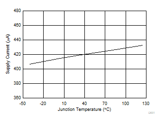
TPS56C230 D001-SupplyCurrent.gif
VEN = 5 V
Figure 1. Supply Current vs Junction Temperature
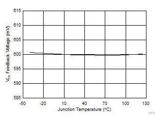
TPS56C230 D003-VFB.gif
Figure 3. Feedback Voltage vs Junction Temperature
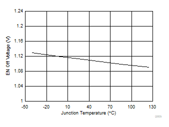
TPS56C230 D005-ENoff.gif
Figure 5. Enable Off Voltage vs Junction Temperature
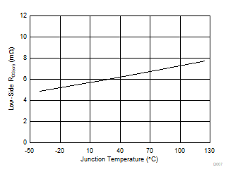
TPS56C230 D007-RDSL.gif
Figure 7. Low-Side RDS(on) vs Junction Temperature
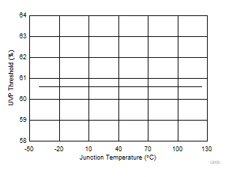
TPS56C230 D009-UVP.gif
Figure 9. UVP Threshold vs Junction Temperature
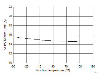
TPS56C230 D011-OC.gif
Figure 11. Valley Current Limit vs Junction Temperature
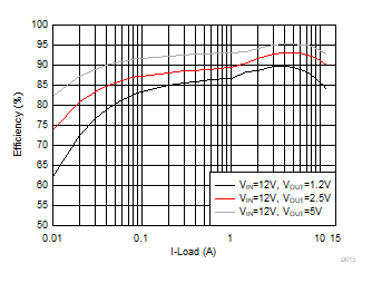
TPS56C230 D013-EfficiencyEco.gif
Figure 13. Efficiency vs Load Current, Eco-mode
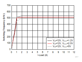
TPS56C230 D017-FswEco.gif
Figure 15. Switching Frequency vs Load Current, Eco-mode
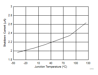
TPS56C230 D002-ShutdownCurrent.gif
VEN = 0 V
Figure 2. Shutdown Current vs Temperature
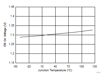
TPS56C230 D004-EN.gif
Figure 4. Enable On Voltage vs Junction Temperature
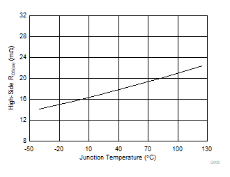
TPS56C230 D006-RDSH.gif
Figure 6. High-Side RDS(on) vs Junction Temperature
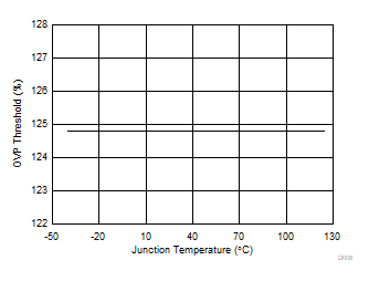
TPS56C230 D008-OVP.gif
Figure 8. OVP Threshold vs Junction Temperature
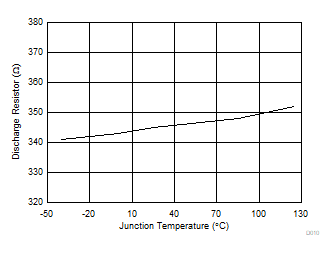
TPS56C230 D010-DischargeR.gif
Figure 10. Discharge Resistor vs Junction Temperature
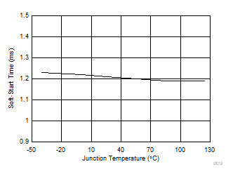
TPS56C230 D012-SSTime.gif
Figure 12. Soft-Start Time vs Junction Temperature
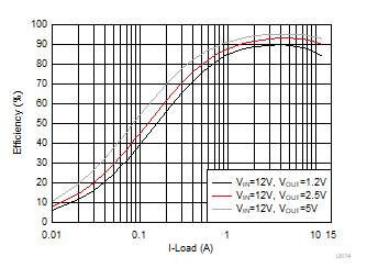
TPS56C230 D014-EfficiencyFccm.gif
Figure 14. Efficiency vs Load Current, FCCM
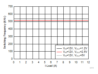
TPS56C230 D018-FswFccm.gif
Figure 16. Switching Frequency vs Load Current, FCCM