-
MSP430F552x、MSP430F551x 混合信号微控制器 ZHCSIR7N March 2009 – September 2018 MSP430F5513 , MSP430F5514 , MSP430F5515 , MSP430F5517 , MSP430F5519 , MSP430F5521 , MSP430F5522 , MSP430F5524 , MSP430F5525 , MSP430F5526 , MSP430F5527 , MSP430F5528 , MSP430F5529
PRODUCTION DATA.
-
MSP430F552x、MSP430F551x 混合信号微控制器
- 1器件概述
- 2修订历史记录
- 3Device Comparison
- 4Terminal Configuration and Functions
-
5Specifications
- 5.1 Absolute Maximum Ratings
- 5.2 ESD Ratings
- 5.3 Recommended Operating Conditions
- 5.4 Active Mode Supply Current Into VCC Excluding External Current
- 5.5 Low-Power Mode Supply Currents (Into VCC) Excluding External Current
- 5.6 Thermal Resistance Characteristics
- 5.7 Schmitt-Trigger Inputs – General-Purpose I/O (P1.0 to P1.7, P2.0 to P2.7, P3.0 to P3.7, P4.0 to P4.7, P5.0 to P5.7, P6.0 to P6.7, P7.0 to P7.7, P8.0 to P8.2, PJ.0 to PJ.3, RST/NMI)
- 5.8 Inputs – Ports P1 and P2 (P1.0 to P1.7, P2.0 to P2.7)
- 5.9 Leakage Current – General-Purpose I/O (P1.0 to P1.7, P2.0 to P2.7, P3.0 to P3.7, P4.0 to P4.7) (P5.0 to P5.7, P6.0 to P6.7, P7.0 to P7.7, P8.0 to P8.2, PJ.0 to PJ.3, RST/NMI)
- 5.10 Outputs – General-Purpose I/O (Full Drive Strength) (P1.0 to P1.7, P2.0 to P2.7, P3.0 to P3.7, P4.0 to P4.7, P5.0 to P5.7, P6.0 to P6.7, P7.0 to P7.7, P8.0 to P8.2, PJ.0 to PJ.3)
- 5.11 Outputs – General-Purpose I/O (Reduced Drive Strength) (P1.0 to P1.7, P2.0 to P2.7, P3.0 to P3.7, P4.0 to P4.7, P5.0 to P5.7, P6.0 to P6.7, P7.0 to P7.7, P8.0 to P8.2, PJ.0 to PJ.3)
- 5.12 Output Frequency – General-Purpose I/O (P1.0 to P1.7, P2.0 to P2.7, P3.0 to P3.7, P4.0 to P4.7, P5.0 to P5.7, P6.0 to P6.7, P7.0 to P7.7, P8.0 to P8.2, PJ.0 to PJ.3)
- 5.13 Typical Characteristics – Outputs, Reduced Drive Strength (PxDS.y = 0)
- 5.14 Typical Characteristics – Outputs, Full Drive Strength (PxDS.y = 1)
- 5.15 Crystal Oscillator, XT1, Low-Frequency Mode
- 5.16 Crystal Oscillator, XT2
- 5.17 Internal Very-Low-Power Low-Frequency Oscillator (VLO)
- 5.18 Internal Reference, Low-Frequency Oscillator (REFO)
- 5.19 DCO Frequency
- 5.20 PMM, Brownout Reset (BOR)
- 5.21 PMM, Core Voltage
- 5.22 PMM, SVS High Side
- 5.23 PMM, SVM High Side
- 5.24 PMM, SVS Low Side
- 5.25 PMM, SVM Low Side
- 5.26 Wake-up Times From Low-Power Modes and Reset
- 5.27 Timer_A
- 5.28 Timer_B
- 5.29 USCI (UART Mode) Clock Frequency
- 5.30 USCI (UART Mode)
- 5.31 USCI (SPI Master Mode) Clock Frequency
- 5.32 USCI (SPI Master Mode)
- 5.33 USCI (SPI Slave Mode)
- 5.34 USCI (I2C Mode)
- 5.35 12-Bit ADC, Power Supply and Input Range Conditions
- 5.36 12-Bit ADC, Timing Parameters
- 5.37 12-Bit ADC, Linearity Parameters Using an External Reference Voltage or AVCC as Reference Voltage
- 5.38 12-Bit ADC, Linearity Parameters Using the Internal Reference Voltage
- 5.39 12-Bit ADC, Temperature Sensor and Built-In VMID
- 5.40 REF, External Reference
- 5.41 REF, Built-In Reference
- 5.42 Comparator_B
- 5.43 Ports PU.0 and PU.1
- 5.44 USB Output Ports DP and DM
- 5.45 USB Input Ports DP and DM
- 5.46 USB-PWR (USB Power System)
- 5.47 USB-PLL (USB Phase-Locked Loop)
- 5.48 Flash Memory
- 5.49 JTAG and Spy-Bi-Wire Interface
-
6Detailed Description
- 6.1 CPU (Link to User's Guide)
- 6.2 Operating Modes
- 6.3 Interrupt Vector Addresses
- 6.4 Memory Organization
- 6.5 Bootloader (BSL)
- 6.6 JTAG Operation
- 6.7 Flash Memory (Link to User's Guide)
- 6.8 RAM (Link to User's Guide)
- 6.9
Peripherals
- 6.9.1 Digital I/O (Link to User's Guide)
- 6.9.2 Port Mapping Controller (Link to User's Guide)
- 6.9.3 Oscillator and System Clock (Link to User's Guide)
- 6.9.4 Power-Management Module (PMM) (Link to User's Guide)
- 6.9.5 Hardware Multiplier (Link to User's Guide)
- 6.9.6 Real-Time Clock (RTC_A) (Link to User's Guide)
- 6.9.7 Watchdog Timer (WDT_A) (Link to User's Guide)
- 6.9.8 System Module (SYS) (Link to User's Guide)
- 6.9.9 DMA Controller (Link to User's Guide)
- 6.9.10 Universal Serial Communication Interface (USCI) (Links to User's Guide: UART Mode, SPI Mode, I2C Mode)
- 6.9.11 TA0 (Link to User's Guide)
- 6.9.12 TA1 (Link to User's Guide)
- 6.9.13 TA2 (Link to User's Guide)
- 6.9.14 TB0 (Link to User's Guide)
- 6.9.15 Comparator_B (Link to User's Guide)
- 6.9.16 ADC12_A (Link to User's Guide)
- 6.9.17 CRC16 (Link to User's Guide)
- 6.9.18 Voltage Reference (REF) Module (Link to User's Guide)
- 6.9.19 Universal Serial Bus (USB) (Link to User's Guide)
- 6.9.20 Embedded Emulation Module (EEM) (Link to User's Guide)
- 6.9.21 Peripheral File Map
- 6.10
Input/Output Diagrams
- 6.10.1 Port P1 (P1.0 to P1.7) Input/Output With Schmitt Trigger
- 6.10.2 Port P2 (P2.0 to P2.7) Input/Output With Schmitt Trigger
- 6.10.3 Port P3 (P3.0 to P3.7) Input/Output With Schmitt Trigger
- 6.10.4 Port P4 (P4.0 to P4.7) Input/Output With Schmitt Trigger
- 6.10.5 Port P5 (P5.0 and P5.1) Input/Output With Schmitt Trigger
- 6.10.6 Port P5 (P5.2 and P5.3) Input/Output With Schmitt Trigger
- 6.10.7 Port P5 (P5.4 and P5.5) Input/Output With Schmitt Trigger
- 6.10.8 Port P5 (P5.6 and P5.7) Input/Output With Schmitt Trigger
- 6.10.9 Port P6 (P6.0 to P6.7) Input/Output With Schmitt Trigger
- 6.10.10 Port P7 (P7.0 to P7.3) Input/Output With Schmitt Trigger
- 6.10.11 Port P7 (P7.4 to P7.7) Input/Output With Schmitt Trigger
- 6.10.12 Port P8 (P8.0 to P8.2) Input/Output With Schmitt Trigger
- 6.10.13 Port PU (PU.0/DP, PU.1/DM, PUR) USB Ports
- 6.10.14 Port PJ (PJ.0) JTAG Pin TDO, Input/Output With Schmitt Trigger or Output
- 6.10.15 Port PJ (PJ.1 to PJ.3) JTAG Pins TMS, TCK, TDI/TCLK, Input/Output With Schmitt Trigger or Output
- 6.11 Device Descriptors (TLV)
- 7器件和文档支持
- 8机械、封装和可订购信息
- 重要声明
MSP430F552x、MSP430F551x 混合信号微控制器
1 器件概述
1.1 特性
- 低电源电压范围:
从 3.6V 低至 1.8V - 超低功耗
- 激活模式 (AM):
- 所有系统时钟激活:
- 8MHz 时为 290µA/MHz、3.0V、闪存程序执行(典型值)
- 8MHz 时为 150µA/MHz、3.0V、RAM 程序执行(典型值)
- 所有系统时钟激活:
- 待机模式 (LPM3):
- 含晶体的实时时钟 (RTC)、看门狗、电源监控器可用、完全 RAM 保持、快速唤醒:
- 2.2V 时为 1.9µA,3.0V 时为 2.1µA(典型值)
- 低功耗振荡器 (VLO)、通用计数器、看门狗、电源监控器可用、完全 RAM 保持、快速唤醒:
- 3.0V 时为 1.4µA(典型值)
- 含晶体的实时时钟 (RTC)、看门狗、电源监控器可用、完全 RAM 保持、快速唤醒:
- 关闭模式 (LPM4):
- 完全 RAM 保持、电源监视器可用、快速唤醒:
- 3.0V 时为 1.1µA(典型值)
- 完全 RAM 保持、电源监视器可用、快速唤醒:
- 关断模式 (LPM4.5):
- 3.0V 时为 0.18µA(典型值)
- 激活模式 (AM):
- 在 3.5µs(典型值)内从待机模式唤醒
- 16 位精简指令集计算机 (RISC) 架构,扩展内存,高达 25MHz 的系统时钟
- 灵活的电源管理系统
- 内置可编程的低压降稳压器 (LDO)
- 电源电压监控、监视和临时限电
- 统一时钟系统
- 针对频率稳定的锁相环 (FLL) 控制环路
- 低功耗低频内部时钟源 (VLO)
- 低频修整内部基准源 (REFO)
- 32kHz 手表晶振 (XT1)
- 高达 32MHz 的高频晶振 (XT2)
- 具有 5 个捕捉/比较寄存器的 16 位定时器 TA0,Timer_A
- 具有 3 个捕捉/比较寄存器的 16 位定时器 TA1,Timer_A
- 具有 3 个捕捉/比较寄存器的 16 位定时器 TA2,Timer_A
- 具有 7 个捕捉/比较影子寄存器的 16 位定时器 TB0,Timer_B
- 2 个通用串行通信接口
- USCI_A0 和 USCI_A1 均支持:
- 增强型通用异步收发器 (UART) 支持自动波特率检测
- IrDA 编码和解码
- 同步串行外设接口 (SPI)
- USCI_B0 和 USCI_B1 每个都支持:
- I2C
- 同步串行外设接口 (SPI)
- USCI_A0 和 USCI_A1 均支持:
- 全速通用串行总线 (USB)
- 集成的 USB - 物理层 (PHY)
- 集成 3.3V 和 1.8V USB 电源系统
- 集成 USB- 锁相环 (PLL)
- 8 输入和 8 输出端点
- 具有内部基准、采样保持和自动扫描功能的 12 位模数转换器 (ADC)(仅限 MSP430F552x)
- 比较器
- 硬件乘法器支持 32 位运算
- 串行板上编程,无需外部编程电压
- 3 通道内部 DMA
- 具有 RTC 特性的基本计时器
- 器件比较 总结了可用的系列产品成员
1.2 应用范围
- 模拟和数字传感器系统
- 数据记录器
- 连接到 USB 主机
1.3 说明
TI 的 MSP430™系列的超低功耗微控制器包含数个采用外设集的器件,可广泛应用于各种 应用。此架构与多种低功耗模式配合使用,是延长便携式测量应用电池寿命的最优 选择。该微控制器 具有 一个强大的 16 位精简指令集 (RISC) CPU,使用 16 位寄存器以及常数发生器,以便获得最高编码效率。此数控振荡器 (DCO) 可使器件在 3.5µs(典型值)内从低功耗模式唤醒至激活模式。
MSP430F5529、MSP430F5527、MSP430F5525 和 MSP430F5521 微控制器具有支持 USB 2.0 的集成 USB 和 PHY、4 个 16 位计时器、1 个高性能 12 位模数转换器 (ADC)、2 个 USCI、1 个硬件乘法器、DMA、1 个带有警报功能的 RTC 模块和 63 个 I/O 引脚。MSP430F5528、MSP430F5526、MSP430F5524 和 MSP430F5522 微控制器包含同样的外设,但具有 47 个 I/O 引脚。
MSP430F5519、MSP430F5517 和 MSP430F5515 微控制器具有支持 USB 2.0 的集成 USB 和 PHY、4 个 16 位计时器、2 个 USCI、1 个硬件乘法器、DMA、1 个带有警报功能的 RTC 模块和 63 个 I/O 引脚。MSP430F5514 和 MSP430FF5513 微控制器包含同样的外设,但具有 47 个 I/O 引脚。
典型 应用 包括需要与多种 USB 主机连接的模拟和数字传感器系统、数据记录器和其它应用。
要获得完整的模块说明,请参阅《MSP430F5xx 和 MSP430F6xx 系列用户指南》
1.4 功能方框图
Figure 1-1 展示了采用 PN 封装的 MSP430F5529、MSP430F5527、MSP430F5525 和 MSP430F5521 器件的功能方框图。
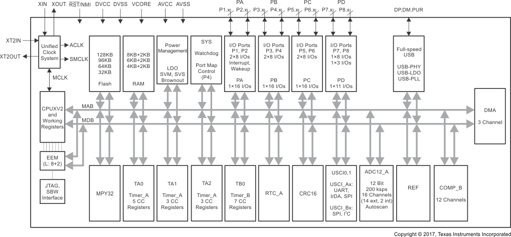 Figure 1-1 功能方框图 – MSP430F5529IPN、MSP430F5527IPN、MSP430F5525IPN、MSP430F5521IPN
 Figure 1-2 展示了采用 RGC 和 ZQE 封装的 MSP430F5528、MSP430F5526、MSP430F5524 和 MSP430F5522 器件的功能方框图,以及采用 YFF 封装的 MSP430F5528、MSP430F5526 和 MSP430F5524 器件的功能方框图。
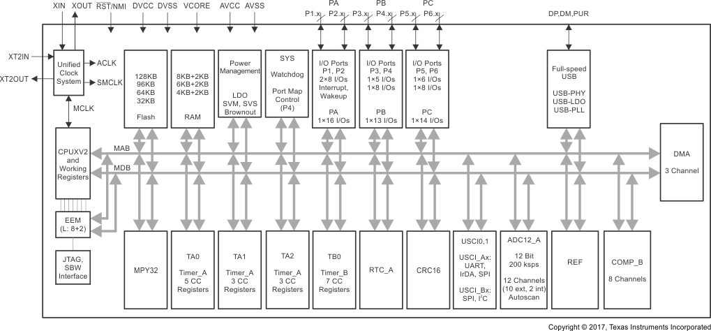 Figure 1-2 功能方框图 –
MSP430F5528IRGC、MSP430F5526IRGC、MSP430F5524IRGC、MSP430F5522IRGC
MSP430F5528IZQE、MSP430F5526IZQE、MSP430F5524IZQE、MSP430F5522IZQE
MSP430F5528IYFF、MSP430F5526IYFF、MSP430F5524IYFF
Figure 1-3 展示了采用 PN 封装的 MSP430F5519、MSP430F5517 和 MSP430F5515 器件的功能方框图。
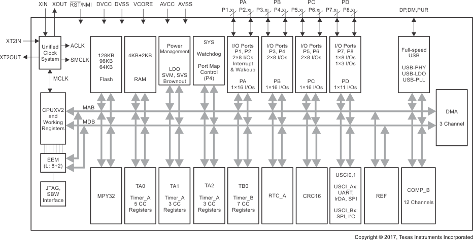 Figure 1-3 功能方框图 – MSP430F5519IPN、MSP430F5517IPN、MSP430F5515IPN
 Figure 1-4 展示了采用 RGC 和 ZQE 封装的 MSP430F5514 和 MSP430F5513 器件的功能方框图。
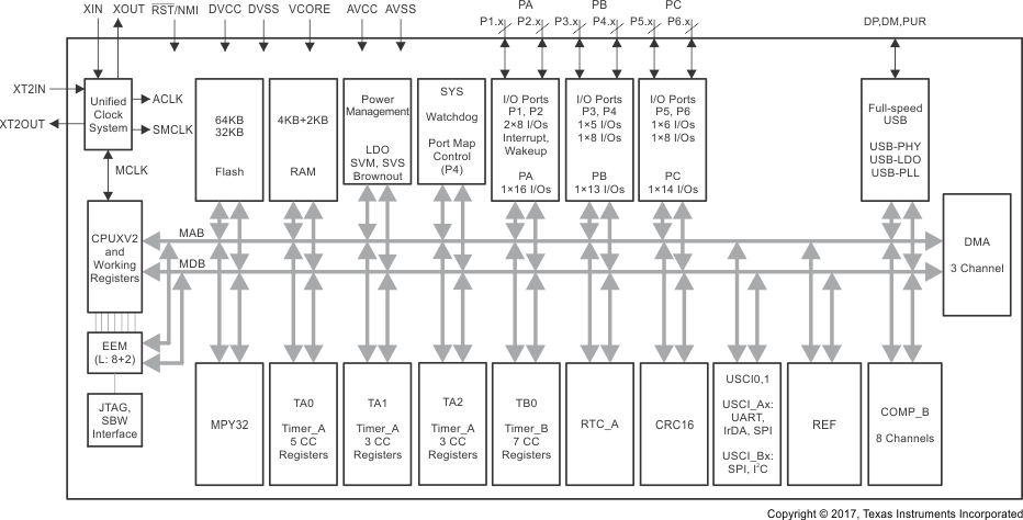 Figure 1-4 功能方框图 – MSP430F5514IRGC、MSP430F5513IRGC、MSP430F5514IZQE、MSP430F5513IZQE
 2 修订历史记录
Changes from November 3, 2015 to September 20, 2018
- 更改了器件信息 表中 DSBGA 封装的封装尺寸条目Go
- Added Section 3.1, Related ProductsGo
- Removed D and E dimension lines from the YFF pinout (for package dimensions, see the Mechanical Data in Section 8)Go
- Added typical conditions statements at the beginning of Section 5, SpecificationsGo
- Changed the MIN value of the V(DVCC_BOR_hys) parameter from 60 mV to 50 mV in Section 5.20, PMM, Brownout Reset (BOR)Go
- Updated notes (1) and (2) and added note (3) in Section 5.26, Wake-up Times From Low-Power Modes and ResetGo
- Removed ADC12DIV from the formula for the TYP value in the second row of the tCONVERT parameter in Section 5.36, 12-Bit ADC, Timing Parameters, because ADC12CLK is after divisionGo
- Added second row for tEN_CMP with Test Conditions of "CBPWRMD = 10" and MAX value of 100 µs in Section 5.42, Comparator_BGo
- Renamed FCTL4.MGR0 and MGR1 bits in the fMCLK,MGR parameter in Section 5.48, Flash Memory, to be consistent with header filesGo
- Throughout document, changed all instances of "bootstrap loader" to "bootloader"Go
- Added YFF pin numbers to Table 6-11, TA0 Signal ConnectionsGo
- Added YFF pin numbers to Table 6-12, TA1 Signal ConnectionsGo
- Added YFF pin numbers to Table 6-13, TA2 Signal ConnectionsGo
- 已将先前的“开发工具支持”部分替换为“Section 7.3、工具与软件”Go
- 更改了格式并添加内容至Section 7.4文档支持Go
3 Device Comparison
Table 3-1 summarizes the available family members.
Table 3-1 Device Comparison(1)(2)
| DEVICE | FLASH
(KB) |
SRAM
(KB)(5) |
Timer_A(3) | Timer_B(4) | USCI | ADC12_A
(Ch) |
COMP_B
(Ch) |
I/Os | PACKAGE | |
|---|---|---|---|---|---|---|---|---|---|---|
| CHANNEL A:
UART, IrDA, SPI |
CHANNEL B:
SPI, I2C |
|||||||||
| MSP430F5529 | 128 | 8 + 2 | 5, 3, 3 | 7 | 2 | 2 | 14 ext, 2 int | 12 | 63 | 80 PN |
| MSP430F5528 | 128 | 8 + 2 | 5, 3, 3 | 7 | 2 | 2 | 10 ext, 2 int | 8 | 47 | 64 RGC, 64 YFF, 80 ZQE |
| MSP430F5527 | 96 | 6 + 2 | 5, 3, 3 | 7 | 2 | 2 | 14 ext, 2 int | 12 | 63 | 80 PN |
| MSP430F5526 | 96 | 6 + 2 | 5, 3, 3 | 7 | 2 | 2 | 10 ext, 2 int | 8 | 47 | 64 RGC, 64 YFF, 80 ZQE |
| MSP430F5525 | 64 | 4 + 2 | 5, 3, 3 | 7 | 2 | 2 | 14 ext, 2 int | 12 | 63 | 80 PN |
| MSP430F5524 | 64 | 4 + 2 | 5, 3, 3 | 7 | 2 | 2 | 10 ext, 2 int | 8 | 47 | 64 RGC, 64 YFF, 80 ZQE |
| MSP430F5522 | 32 | 8 + 2 | 5, 3, 3 | 7 | 2 | 2 | 10 ext, 2 int | 8 | 47 | 64 RGC, 80 ZQE |
| MSP430F5521 | 32 | 6 + 2 | 5, 3, 3 | 7 | 2 | 2 | 14 ext, 2 int | 12 | 63 | 80 PN |
| MSP430F5519 | 128 | 8 + 2 | 5, 3, 3 | 7 | 2 | 2 | – | 12 | 63 | 80 PN |
| MSP430F5517 | 96 | 6 + 2 | 5, 3, 3 | 7 | 2 | 2 | – | 12 | 63 | 80 PN |
| MSP430F5515 | 64 | 4 + 2 | 5, 3, 3 | 7 | 2 | 2 | – | 12 | 63 | 80 PN |
| MSP430F5514 | 64 | 4 + 2 | 5, 3, 3 | 7 | 2 | 2 | – | 8 | 47 | 64 RGC, 80 ZQE |
| MSP430F5513 | 32 | 4 + 2 | 5, 3, 3 | 7 | 2 | 2 | – | 8 | 47 | 64 RGC, 80 ZQE |
3.1 Related Products
For information about other devices in this family of products or related products, see the following links.
- Products for TI Microcontrollers
TI's low-power and high-performance MCUs, with wired and wireless connectivity options, are optimized for a broad range of applications.
- Products for MSP430 Ultra-Low-Power Microcontrollers
One platform. One ecosystem. Endless possibilities. Enabling the connected world with innovations in ultra-low-power microcontrollers with advanced peripherals for precise sensing and measurement.
- Companion Products for MSP430F5529
Review products that are frequently purchased or used with this product.
- Reference Designs for MSP430F5529
The TI Designs Reference Design Library is a robust reference design library that spans analog, embedded processor, and connectivity. Created by TI experts to help you jump start your system design, all TI Designs include schematic or block diagrams, BOMs, and design files to speed your time to market.
4 Terminal Configuration and Functions
4.1 Pin Diagrams
Figure 4-1 shows the pinout for the MSP430F5529, MSP430F5527, MSP430F5525, and MSP430F5521 devices in the 80-pin PN package.
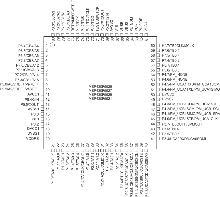 Figure 4-1 80-Pin PN Package – MSP430F5529IPN, MSP430F5527IPN, MSP430F5525IPN, MSP430F5521IPN (Top View)
 Figure 4-2 shows the pinout for the MSP430F5528, MSP430F5526, MSP430F5524, and MSP430F5522 devices in the 64-pin RGC package.
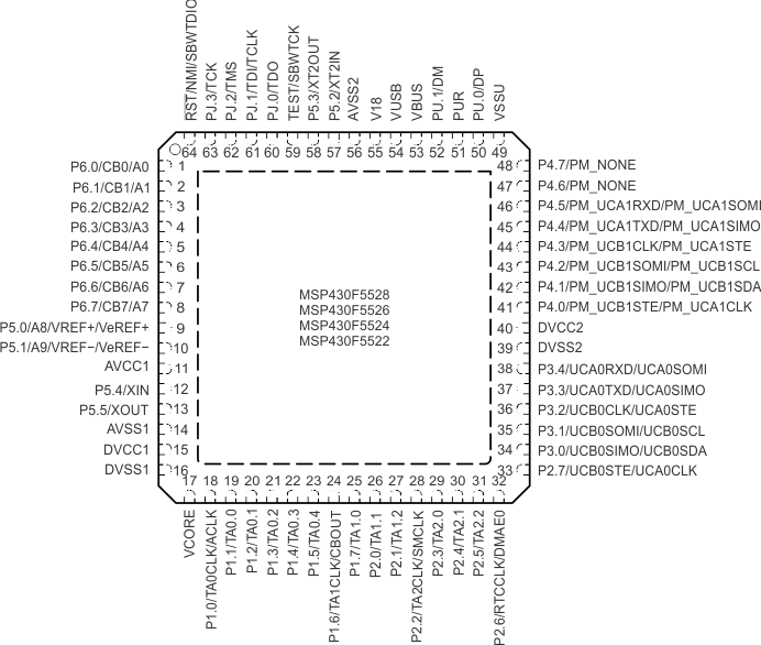
NOTE:
TI recommends connecting the exposed thermal pad to VSS.Figure 4-3 shows the pinout for the MSP430F5519, MSP430F5517, and MSP430F5515 devices in the 80-pin PN package.
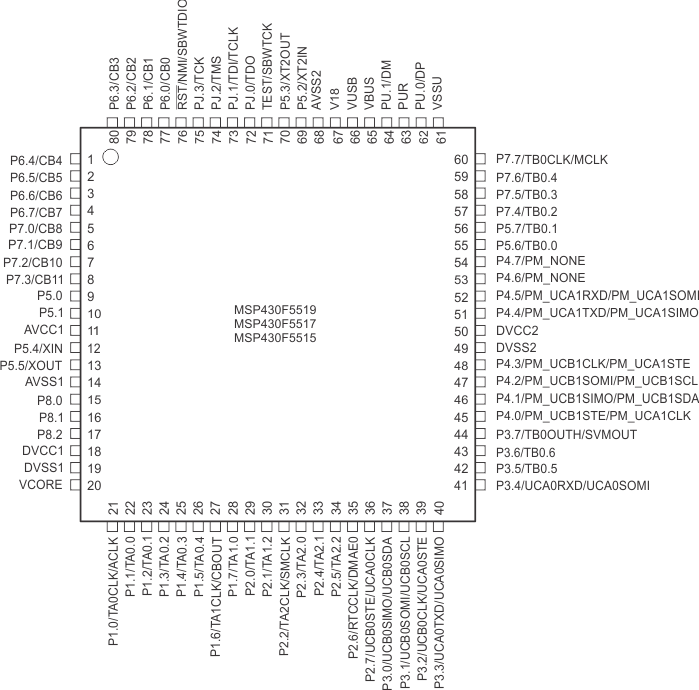 Figure 4-3 80-Pin PN Package – MSP430F5519IPN, MSP430F5517IPN, MSP430F5515IPN (Top View)
 Figure 4-4 shows the pinout for the MSP430F5514 and MSP430F5513 devices in the 64-pin RGC package.
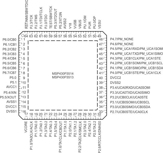
NOTE:
TI recommends connecting the exposed thermal pad to VSS.Figure 4-5 shows the pinout for the MSP430F5528, MSP430F5526, MSP430F5524, MSP430F5522, MSP430F5514, and MSP430F5513 devices in the 80-pin ZQE package.
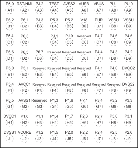 Figure 4-5 80-Pin ZQE Package – MSP430F5528IZQE, MSP430F5526IZQE, MSP430F5524IZQE, MSP430F5522IZQE, MSP430F5514IZQE, MSP430F5513IZQE (Top View)
 Figure 4-6 shows the pinout for the MSP430F5528, MSP430F5526, and MSP430F5524 devices in the 64-pin YFF package. For package dimensions, see the Mechanical Data in Section 8.
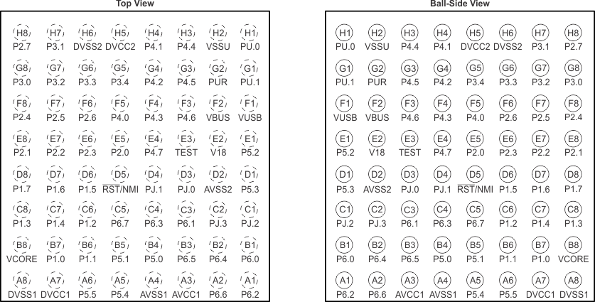 Figure 4-6 64-Pin YFF Package – MSP430F5528IYFF, MSP430F5526IYFF, MSP430F5524IYFF
 4.2 Signal Descriptions
Table 4-1 describes the signals for all device and package options.
Table 4-1 Terminal Functions
| TERMINAL | I/O(1) | DESCRIPTION | ||||
|---|---|---|---|---|---|---|
| NAME | NO. | |||||
| PN | RGC | YFF | ZQE | |||
| P6.4/CB4/A4 | 1 | 5 | B2 | C1 | I/O | General-purpose digital I/O |
| Comparator_B input CB4 | ||||||
| Analog input A4 for ADC (not available on F551x devices) | ||||||
| P6.5/CB5/A5 | 2 | 6 | B3 | D2 | I/O | General-purpose digital I/O |
| Comparator_B input CB5 | ||||||
| Analog input A5 for ADC (not available on F551x devices) | ||||||
| P6.6/CB6/A6 | 3 | 7 | A2 | D1 | I/O | General-purpose digital I/O |
| Comparator_B input CB6 | ||||||
| Analog input A6 for ADC (not available on F551x devices) | ||||||
| P6.7/CB7/A7 | 4 | 8 | C5 | D3 | I/O | General-purpose digital I/O |
| Comparator_B input CB7 | ||||||
| Analog input A7 for ADC (not available on F551x devices) | ||||||
| P7.0/CB8/A12 | 5 | N/A | N/A | N/A | I/O | General-purpose digital I/O (not available on F5528, F5526, F5524, F5522, F5514, F5513 devices) |
| Comparator_B input CB8 (not available on F5528, F5526, F5524, F5522, F5514, F5513 devices) | ||||||
| Analog input A12 for ADC (not available on F551x devices) | ||||||
| P7.1/CB9/A13 | 6 | N/A | N/A | N/A | I/O | General-purpose digital I/O (not available on F5528, F5526, F5524, F5522, F5514, F5513 devices) |
| Comparator_B input CB9 (not available on F5528, F5526, F5524, F5522, F5514, F5513 devices) | ||||||
| Analog input A13 for ADC (not available on F551x devices) | ||||||
| P7.2/CB10/A14 | 7 | N/A | N/A | N/A | I/O | General-purpose digital I/O (not available on F5528, F5526, F5524, F5522, F5514, F5513 devices) |
| Comparator_B input CB10 (not available on F5528, F5526, F5524, F5522, F5514, F5513 devices) | ||||||
| Analog input A14 for ADC (not available on F551x devices) | ||||||
| P7.3/CB11/A15 | 8 | N/A | N/A | N/A | I/O | General-purpose digital I/O (not available on F5528, F5526, F5524, F5522, F5514, F5513 devices) |
| Comparator_B input CB11 (not available on F5528, F5526, F5524, F5522, F5514, F5513 devices) | ||||||
| Analog input A15 for ADC (not available on F551x devices) | ||||||
| P5.0/A8/VREF+/VeREF+ | 9 | 9 | B4 | E1 | I/O | General-purpose digital I/O |
| Output of reference voltage to the ADC (not available on F551x devices) | ||||||
| Input for an external reference voltage to the ADC (not available on F551x devices) | ||||||
| Analog input A8 for ADC (not available on F551x devices) | ||||||
| P5.1/A9/VREF-/VeREF- | 10 | 10 | B5 | E2 | I/O | General-purpose digital I/O |
| Negative terminal for the ADC reference voltage for both sources, the internal reference voltage, or an external applied reference voltage (not available on F551x devices) | ||||||
| Analog input A9 for ADC (not available on F551x devices) | ||||||
| AVCC1 | 11 | 11 | A3 | F2 | Analog power supply | |
| P5.4/XIN | 12 | 12 | A5 | F1 | I/O | General-purpose digital I/O |
| Input terminal for crystal oscillator XT1 | ||||||
| P5.5/XOUT | 13 | 13 | A6 | G1 | I/O | General-purpose digital I/O |
| Output terminal of crystal oscillator XT1 | ||||||
| AVSS1 | 14 | 14 | A4 | G2 | Analog ground supply | |
| P8.0 | 15 | N/A | N/A | N/A | I/O | General-purpose digital I/O |
| P8.1 | 16 | N/A | N/A | N/A | I/O | General-purpose digital I/O |
| P8.2 | 17 | N/A | N/A | N/A | I/O | General-purpose digital I/O |
| DVCC1 | 18 | 15 | A7 | H1 | Digital power supply | |
| DVSS1 | 19 | 16 | A8 | J1 | Digital ground supply | |
| VCORE(3) | 20 | 17 | B8 | J2 | Regulated core power supply output (internal use only, no external current loading) | |
| P1.0/TA0CLK/ACLK | 21 | 18 | B7 | H2 | I/O | General-purpose digital I/O with port interrupt |
| TA0 clock signal TA0CLK input | ||||||
| ACLK output (divided by 1, 2, 4, 8, 16, or 32) | ||||||
| P1.1/TA0.0 | 22 | 19 | B6 | H3 | I/O | General-purpose digital I/O with port interrupt |
| TA0 CCR0 capture: CCI0A input, compare: Out0 output | ||||||
| BSL transmit output | ||||||
| P1.2/TA0.1 | 23 | 20 | C6 | J3 | I/O | General-purpose digital I/O with port interrupt |
| TA0 CCR1 capture: CCI1A input, compare: Out1 output | ||||||
| BSL receive input | ||||||
| P1.3/TA0.2 | 24 | 21 | C8 | G4 | I/O | General-purpose digital I/O with port interrupt |
| TA0 CCR2 capture: CCI2A input, compare: Out2 output | ||||||
| P1.4/TA0.3 | 25 | 22 | C7 | H4 | I/O | General-purpose digital I/O with port interrupt |
| TA0 CCR3 capture: CCI3A input compare: Out3 output | ||||||
| P1.5/TA0.4 | 26 | 23 | D6 | J4 | I/O | General-purpose digital I/O with port interrupt |
| TA0 CCR4 capture: CCI4A input, compare: Out4 output | ||||||
| P1.6/TA1CLK/CBOUT | 27 | 24 | D7 | G5 | I/O | General-purpose digital I/O with port interrupt |
| TA1 clock signal TA1CLK input | ||||||
| Comparator_B output | ||||||
| P1.7/TA1.0 | 28 | 25 | D8 | H5 | I/O | General-purpose digital I/O with port interrupt |
| TA1 CCR0 capture: CCI0A input, compare: Out0 output | ||||||
| P2.0/TA1.1 | 29 | 26 | E5 | J5 | I/O | General-purpose digital I/O with port interrupt |
| TA1 CCR1 capture: CCI1A input, compare: Out1 output | ||||||
| P2.1/TA1.2 | 30 | 27 | E8 | G6 | I/O | General-purpose digital I/O with port interrupt |
| TA1 CCR2 capture: CCI2A input, compare: Out2 output | ||||||
| P2.2/TA2CLK/SMCLK | 31 | 28 | E7 | J6 | I/O | General-purpose digital I/O with port interrupt |
| TA2 clock signal TA2CLK input | ||||||
| SMCLK output | ||||||
| P2.3/TA2.0 | 32 | 29 | E6 | H6 | I/O | General-purpose digital I/O with port interrupt |
| TA2 CCR0 capture: CCI0A input, compare: Out0 output | ||||||
| P2.4/TA2.1 | 33 | 30 | F8 | J7 | I/O | General-purpose digital I/O with port interrupt |
| TA2 CCR1 capture: CCI1A input, compare: Out1 output | ||||||
| P2.5/TA2.2 | 34 | 31 | F7 | J8 | I/O | General-purpose digital I/O with port interrupt |
| TA2 CCR2 capture: CCI2A input, compare: Out2 output | ||||||
| P2.6/RTCCLK/DMAE0 | 35 | 32 | F6 | J9 | I/O | General-purpose digital I/O with port interrupt |
| RTC clock output for calibration | ||||||
| DMA external trigger input | ||||||
| P2.7/UCB0STE/UCA0CLK | 36 | 33 | H8 | H7 | I/O | General-purpose digital I/O with port interrupt |
| Slave transmit enable – USCI_B0 SPI mode | ||||||
| Clock signal input – USCI_A0 SPI slave mode | ||||||
| Clock signal output – USCI_A0 SPI master mode | ||||||
| P3.0/UCB0SIMO/ UCB0SDA | 37 | 34 | G8 | H8 | I/O | General-purpose digital I/O |
| Slave in, master out – USCI_B0 SPI mode | ||||||
| I2C data – USCI_B0 I2C mode | ||||||
| P3.1/UCB0SOMI/UCB0SCL | 38 | 35 | H7 | H9 | I/O | General-purpose digital I/O |
| Slave out, master in – USCI_B0 SPI mode | ||||||
| I2C clock – USCI_B0 I2C mode | ||||||
| P3.2/UCB0CLK/UCA0STE | 39 | 36 | G7 | G8 | I/O | General-purpose digital I/O |
| Clock signal input – USCI_B0 SPI slave mode | ||||||
| Clock signal output – USCI_B0 SPI master mode | ||||||
| Slave transmit enable – USCI_A0 SPI mode | ||||||
| P3.3/UCA0TXD/ UCA0SIMO | 40 | 37 | G6 | G9 | I/O | General-purpose digital I/O |
| Transmit data – USCI_A0 UART mode | ||||||
| Slave in, master out – USCI_A0 SPI mode | ||||||
| P3.4/UCA0RXD/ UCA0SOMI | 41 | 38 | G5 | G7 | I/O | General-purpose digital I/O |
| Receive data – USCI_A0 UART mode | ||||||
| Slave out, master in – USCI_A0 SPI mode | ||||||
| P3.5/TB0.5 | 42 | N/A | N/A | N/A | I/O | General-purpose digital I/O (not available on F5528, F5526, F5524, F5522, F5514, F5513 devices) |
| TB0 CCR5 capture: CCI5A input, compare: Out5 output | ||||||
| P3.6/TB0.6 | 43 | N/A | N/A | N/A | I/O | General-purpose digital I/O (not available on F5528, F5526, F5524, F5522, F5514, F5513 devices) |
| TB0 CCR6 capture: CCI6A input, compare: Out6 output | ||||||
| P3.7/TB0OUTH/SVMOUT | 44 | N/A | N/A | N/A | I/O | General-purpose digital I/O (not available on F5528, F5526, F5524, F5522, F5514, F5513 devices) |
| Switch all PWM outputs high impedance input – TB0 (not available on F5528, F5526, F5524, F5522, F5514, F5513 devices) | ||||||
| SVM output (not available on F5528, F5526, F5524, F5522, F5514, F5513 devices) | ||||||
| P4.0/PM_UCB1STE/ PM_UCA1CLK | 45 | 41 | F5 | E8 | I/O | General-purpose digital I/O with reconfigurable port mapping secondary function |
| Default mapping: Slave transmit enable – USCI_B1 SPI mode | ||||||
| Default mapping: Clock signal input – USCI_A1 SPI slave mode | ||||||
| Default mapping: Clock signal output – USCI_A1 SPI master mode | ||||||
| P4.1/PM_UCB1SIMO/ PM_UCB1SDA | 46 | 42 | H4 | E7 | I/O | General-purpose digital I/O with reconfigurable port mapping secondary function |
| Default mapping: Slave in, master out – USCI_B1 SPI mode | ||||||
| Default mapping: I2C data – USCI_B1 I2C mode | ||||||
| P4.2/PM_UCB1SOMI/ PM_UCB1SCL | 47 | 43 | G4 | D9 | I/O | General-purpose digital I/O with reconfigurable port mapping secondary function |
| Default mapping: Slave out, master in – USCI_B1 SPI mode | ||||||
| Default mapping: I2C clock – USCI_B1 I2C mode | ||||||
| P4.3/PM_UCB1CLK/ PM_UCA1STE | 48 | 44 | F4 | D8 | I/O | General-purpose digital I/O with reconfigurable port mapping secondary function |
| Default mapping: Clock signal input – USCI_B1 SPI slave mode | ||||||
| Default mapping: Clock signal output – USCI_B1 SPI master mode | ||||||
| Default mapping: Slave transmit enable – USCI_A1 SPI mode | ||||||
| DVSS2 | 49 | 39 | H6 | F9 | Digital ground supply | |
| DVCC2 | 50 | 40 | H5 | E9 | Digital power supply | |
| P4.4/PM_UCA1TXD/ PM_UCA1SIMO | 51 | 45 | H3 | D7 | I/O | General-purpose digital I/O with reconfigurable port mapping secondary function |
| Default mapping: Transmit data – USCI_A1 UART mode | ||||||
| Default mapping: Slave in, master out – USCI_A1 SPI mode | ||||||
| P4.5/PM_UCA1RXD/ PM_UCA1SOMI | 52 | 46 | G3 | C9 | I/O | General-purpose digital I/O with reconfigurable port mapping secondary function |
| Default mapping: Receive data – USCI_A1 UART mode | ||||||
| Default mapping: Slave out, master in – USCI_A1 SPI mode | ||||||
| P4.6/PM_NONE | 53 | 47 | F3 | C8 | I/O | General-purpose digital I/O with reconfigurable port mapping secondary function |
| Default mapping: no secondary function. | ||||||
| P4.7/PM_NONE | 54 | 48 | E4 | C7 | I/O | General-purpose digital I/O with reconfigurable port mapping secondary function |
| Default mapping: no secondary function. | ||||||
| P5.6/TB0.0 | 55 | N/A | N/A | N/A | I/O | General-purpose digital I/O (not available on F5528, F5526, F5524, F5522, F5514, F5513 devices) |
| TB0 CCR0 capture: CCI0A input, compare: Out0 output (not available on F5528, F5526, F5524, F5522, F5514, F5513 devices) | ||||||
| P5.7/TB0.1 | 56 | N/A | N/A | N/A | I/O | General-purpose digital I/O (not available on F5528, F5526, F5524, F5522, F5514, F5513 devices) |
| TB0 CCR1 capture: CCI1A input, compare: Out1 output (not available on F5528, F5526, F5524, F5522, F5514, F5513 devices) | ||||||
| P7.4/TB0.2 | 57 | N/A | N/A | N/A | I/O | General-purpose digital I/O (not available on F5528, F5526, F5524, F5522, F5514, F5513 devices) |
| TB0 CCR2 capture: CCI2A input, compare: Out2 output (not available on F5528, F5526, F5524, F5522, F5514, F5513 devices) | ||||||
| P7.5/TB0.3 | 58 | N/A | N/A | N/A | I/O | General-purpose digital I/O (not available on F5528, F5526, F5524, F5522, F5514, F5513 devices) |
| TB0 CCR3 capture: CCI3A input, compare: Out3 output (not available on F5528, F5526, F5524, F5522, F5514, F5513 devices) | ||||||
| P7.6/TB0.4 | 59 | N/A | N/A | N/A | I/O | General-purpose digital I/O (not available on F5528, F5526, F5524, F5522, F5514, F5513 devices) |
| TB0 CCR4 capture: CCI4A input, compare: Out4 output (not available on F5528, F5526, F5524, F5522, F5514, F5513 devices) | ||||||
| P7.7/TB0CLK/MCLK | 60 | N/A | N/A | N/A | I/O | General-purpose digital I/O (not available on F5528, F5526, F5524, F5522, F5514, F5513 devices) |
| TB0 clock signal TBCLK input (not available on F5528, F5526, F5524, F5522, F5514, F5513 devices) | ||||||
| MCLK output (not available on F5528, F5526, F5524, F5522, F5514, F5513 devices) | ||||||
| VSSU | 61 | 49 | H2 | B8, B9 | USB PHY ground supply | |
| PU.0/DP | 62 | 50 | H1 | A9 | I/O | General-purpose digital I/O. Controlled by USB control register |
| USB data terminal DP | ||||||
| PUR | 63 | 51 | G2 | B7 | I/O | USB pullup resistor pin (open drain). The voltage level at the PUR pin is used to invoke the default USB BSL. Recommended 1-MΩ resistor to ground. See Section 6.5.1 for more information. |
| PU.1/DM | 64 | 52 | G1 | A8 | I/O | General-purpose digital I/O. Controlled by USB control register |
| USB data terminal DM | ||||||
| VBUS | 65 | 53 | F2 | A7 | USB LDO input (connect to USB power source) | |
| VUSB | 66 | 54 | F1 | A6 | USB LDO output | |
| V18 | 67 | 55 | E2 | B6 | USB regulated power (internal use only, no external current loading) | |
| AVSS2 | 68 | 56 | D2 | A5 | Analog ground supply | |
| P5.2/XT2IN | 69 | 57 | E1 | B5 | I/O | General-purpose digital I/O |
| Input terminal for crystal oscillator XT2 | ||||||
| P5.3/XT2OUT | 70 | 58 | D1 | B4 | I/O | General-purpose digital I/O |
| Output terminal of crystal oscillator XT2 | ||||||
| TEST/SBWTCK(4) | 71 | 59 | E3 | A4 | I | Test mode pin – selects 4-wire JTAG operation |
| Spy-Bi-Wire input clock when Spy-Bi-Wire operation activated | ||||||
| PJ.0/TDO(5) | 72 | 60 | D3 | C5 | I/O | General-purpose digital I/O |
| JTAG test data output port | ||||||
| PJ.1/TDI/TCLK(5) | 73 | 61 | D4 | C4 | I/O | General-purpose digital I/O |
| JTAG test data input | ||||||
| Test clock input | ||||||
| PJ.2/TMS(5) | 74 | 62 | C1 | A3 | I/O | General-purpose digital I/O |
| JTAG test mode select | ||||||
| PJ.3/TCK(5) | 75 | 63 | C2 | B3 | I/O | General-purpose digital I/O |
| JTAG test clock | ||||||
| RST/NMI/SBWTDIO(4) | 76 | 64 | D5 | A2 | I/O | Reset input, active low(6) |
| Nonmaskable interrupt input | ||||||
| Spy-Bi-Wire data input/output when Spy-Bi-Wire operation activated | ||||||
| P6.0/CB0/A0 | 77 | 1 | B1 | A1 | I/O | General-purpose digital I/O |
| Comparator_B input CB0 | ||||||
| Analog input A0 for ADC (not available on F551x devices) | ||||||
| P6.1/CB1/A1 | 78 | 2 | C3 | B2 | I/O | General-purpose digital I/O |
| Comparator_B input CB1 | ||||||
| Analog input A1 for ADC (not available on F551x devices) | ||||||
| P6.2/CB2/A2 | 79 | 3 | A1 | B1 | I/O | General-purpose digital I/O |
| Comparator_B input CB2 | ||||||
| Analog input A2 for ADC (not available on F551x devices) | ||||||
| P6.3/CB3/A3 | 80 | 4 | C4 | C2 | I/O | General-purpose digital I/O |
| Comparator_B input CB3 | ||||||
| Analog input A3 for ADC (not available on F551x devices) | ||||||
| Reserved | N/A | N/A | N/A | (2) | Reserved. Connect to ground. | |
| QFN Pad | N/A | Pad | N/A | N/A | QFN package pad. TI recommends connecting to VSS. | |
5.1 Absolute Maximum Ratings
over operating free-air temperature range (unless otherwise noted)(1)| MIN | MAX | UNIT | |
|---|---|---|---|
| Voltage applied at VCC to VSS | –0.3 | 4.1 | V |
| Voltage applied to any pin (excluding VCORE, VBUS, V18)(2) | –0.3 | VCC + 0.3 | V |
| Diode current at any device pin | ±2 | mA | |
| Maximum operating junction temperature, TJ | 95 | °C | |
| Storage temperature, Tstg(3) | –55 | 150 | °C |
5.2 ESD Ratings
| VALUE | UNIT | |||
|---|---|---|---|---|
| V(ESD) | Electrostatic discharge | Human-body model (HBM), per ANSI/ESDA/JEDEC JS-001(1) | ±1000 | V |
| Charged-device model (CDM), per JEDEC specification JESD22-C101(2) | ±250 | |||
5.3 Recommended Operating Conditions
| MIN | NOM | MAX | UNIT | |||
|---|---|---|---|---|---|---|
| VCC | Supply voltage during program execution and flash programming (AVCC = DVCC1 = DVCC2 = DVCC)(1)(3) | PMMCOREVx = 0 | 1.8 | 3.6 | V | |
| PMMCOREVx = 0, 1 | 2.0 | 3.6 | ||||
| PMMCOREVx = 0, 1, 2 | 2.2 | 3.6 | ||||
| PMMCOREVx = 0, 1, 2, 3 | 2.4 | 3.6 | ||||
| VCC, USB | Supply voltage during USB operation, USB PLL disabled,
USB_EN = 1, UPLLEN = 0 |
PMMCOREVx = 0 | 1.8 | 3.6 | V | |
| PMMCOREVx = 0, 1 | 2.0 | 3.6 | ||||
| PMMCOREVx = 0, 1, 2 | 2.2 | 3.6 | ||||
| PMMCOREVx = 0, 1, 2, 3 | 2.4 | 3.6 | ||||
| Supply voltage during USB operation, USB PLL enabled(5),
USB_EN = 1, UPLLEN = 1 |
PMMCOREVx = 2 | 2.2 | 3.6 | |||
| PMMCOREVx = 2, 3 | 2.4 | 3.6 | ||||
| VSS | Supply voltage (AVSS = DVSS1 = DVSS2 = DVSS) | 0 | V | |||
| TA | Operating free-air temperature | I version | –40 | 85 | °C | |
| TJ | Operating junction temperature | I version | –40 | 85 | °C | |
| CVCORE | Recommended capacitor at VCORE(2) | 470 | nF | |||
| CDVCC/ CVCORE | Capacitor ratio of DVCC to VCORE | 10 | ratio | |||
| fSYSTEM | Processor frequency (maximum MCLK frequency)(4) (see Figure 5-1) | PMMCOREVx = 0,
1.8 V ≤ VCC ≤ 3.6 V (default condition) |
0 | 8.0 | MHz | |
| PMMCOREVx = 1,
2.0 V ≤ VCC ≤ 3.6 V |
0 | 12.0 | ||||
| PMMCOREVx = 2,
2.2 V ≤ VCC ≤ 3.6 V |
0 | 20.0 | ||||
| PMMCOREVx = 3,
2.4 V ≤ VCC ≤ 3.6 V |
0 | 25.0 | ||||
| fSYSTEM_USB | Minimum processor frequency for USB operation | 1.5 | MHz | |||
| USB_wait | Wait state cycles during USB operation | 16 | cycles | |||
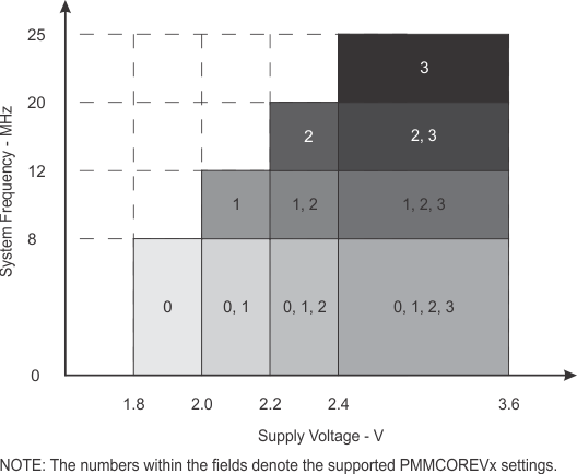 Figure 5-1 Maximum System Frequency
 5.4 Active Mode Supply Current Into VCC Excluding External Current
over recommended operating free-air temperature (unless otherwise noted)(1)(2)(3)| PARAMETER | EXECUTION MEMORY | VCC | PMMCOREVx | FREQUENCY (fDCO = fMCLK = fSMCLK) | UNIT | |||||||||
|---|---|---|---|---|---|---|---|---|---|---|---|---|---|---|
| 1 MHz | 8 MHz | 12 MHz | 20 MHz | 25 MHz | ||||||||||
| TYP | MAX | TYP | MAX | TYP | MAX | TYP | MAX | TYP | MAX | |||||
| IAM, Flash | Flash | 3.0 V | 0 | 0.36 | 0.47 | 2.32 | 2.60 | mA | ||||||
| 1 | 0.40 | 2.65 | 4.0 | 4.4 | ||||||||||
| 2 | 0.44 | 2.90 | 4.3 | 7.1 | 7.7 | |||||||||
| 3 | 0.46 | 3.10 | 4.6 | 7.6 | 10.1 | 11.0 | ||||||||
| IAM, RAM | RAM | 3.0 V | 0 | 0.20 | 0.24 | 1.20 | 1.30 | mA | ||||||
| 1 | 0.22 | 1.35 | 2.0 | 2.2 | ||||||||||
| 2 | 0.24 | 1.50 | 2.2 | 3.7 | 4.2 | |||||||||
| 3 | 0.26 | 1.60 | 2.4 | 3.9 | 5.3 | 6.2 | ||||||||
fACLK = 32786 Hz, fDCO = fMCLK = fSMCLK at specified frequency.
XTS = CPUOFF = SCG0 = SCG1 = OSCOFF= SMCLKOFF = 0.
5.5 Low-Power Mode Supply Currents (Into VCC) Excluding External Current
over recommended ranges of supply voltage and operating free-air temperature (unless otherwise noted)(1)(2)| PARAMETER | VCC | PMMCOREVx | –40°C | 25°C | 60°C | 85°C | UNIT | |||||
|---|---|---|---|---|---|---|---|---|---|---|---|---|
| TYP | MAX | TYP | MAX | TYP | MAX | TYP | MAX | |||||
| ILPM0,1MHz | Low-power mode 0(3)(9) | 2.2 V | 0 | 73 | 77 | 85 | 80 | 85 | 97 | µA | ||
| 3.0 V | 3 | 79 | 83 | 92 | 88 | 95 | 105 | |||||
| ILPM2 | Low-power mode 2(4)(9) | 2.2 V | 0 | 6.5 | 6.5 | 12 | 10 | 11 | 17 | µA | ||
| 3.0 V | 3 | 7.0 | 7.0 | 13 | 11 | 12 | 18 | |||||
| ILPM3,XT1LF | Low-power mode 3, crystal mode(5)(9) | 2.2 V | 0 | 1.60 | 1.90 | 2.6 | 5.6 | µA | ||||
| 1 | 1.65 | 2.00 | 2.7 | 5.9 | ||||||||
| 2 | 1.75 | 2.15 | 2.9 | 6.1 | ||||||||
| 3.0 V | 0 | 1.8 | 2.1 | 2.9 | 2.8 | 5.8 | 8.3 | |||||
| 1 | 1.9 | 2.3 | 2.9 | 6.1 | ||||||||
| 2 | 2.0 | 2.4 | 3.0 | 6.3 | ||||||||
| 3 | 2.0 | 2.5 | 3.9 | 3.1 | 6.4 | 9.3 | ||||||
| ILPM3,VLO | Low-power mode 3, VLO mode(6)(9) | 3.0 V | 0 | 1.1 | 1.4 | 2.7 | 1.9 | 4.9 | 7.4 | µA | ||
| 1 | 1.1 | 1.4 | 2.0 | 5.2 | ||||||||
| 2 | 1.2 | 1.5 | 2.1 | 5.3 | ||||||||
| 3 | 1.3 | 1.6 | 3.0 | 2.2 | 5.4 | 8.5 | ||||||
| ILPM4 | Low-power mode 4(7)(9) | 3.0 V | 0 | 0.9 | 1.1 | 1.5 | 1.8 | 4.8 | 7.3 | µA | ||
| 1 | 1.1 | 1.2 | 2.0 | 5.1 | ||||||||
| 2 | 1.2 | 1.2 | 2.1 | 5.2 | ||||||||
| 3 | 1.3 | 1.3 | 1.6 | 2.2 | 5.3 | 8.1 | ||||||
| ILPM4.5 | Low-power mode 4.5(8) | 3.0 V | 0.15 | 0.18 | 0.35 | 0.26 | 0.5 | 1.0 | µA | |||
CPUOFF = 1, SCG0 = 0, SCG1 = 0, OSCOFF = 0 (LPM0); fACLK = 32768 Hz, fMCLK = 0 MHz, fSMCLK = fDCO = 1 MHz
USB disabled (VUSBEN = 0, SLDOEN = 0).
CPUOFF = 1, SCG0 = 0, SCG1 = 1, OSCOFF = 0 (LPM2); fACLK = 32768 Hz, fMCLK = 0 MHz, fSMCLK = fDCO = 0 MHz; DCO setting = 1 MHz operation, DCO bias generator enabled.
USB disabled (VUSBEN = 0, SLDOEN = 0)
CPUOFF = 1, SCG0 = 1, SCG1 = 1, OSCOFF = 0 (LPM3); fACLK = 32768 Hz, fMCLK = fSMCLK = fDCO = 0 MHz
USB disabled (VUSBEN = 0, SLDOEN = 0)
CPUOFF = 1, SCG0 = 1, SCG1 = 1, OSCOFF = 0 (LPM3); fACLK = fVLO, fMCLK = fSMCLK = fDCO = 0 MHz
USB disabled (VUSBEN = 0, SLDOEN = 0)
USB disabled (VUSBEN = 0, SLDOEN = 0)
CPUOFF = 1, SCG0 = 1, SCG1 = 1, OSCOFF = 1, PMMREGOFF = 1 (LPM4.5); fDCO = fACLK = fMCLK = fSMCLK = 0 MHz
5.6 Thermal Resistance Characteristics
| THERMAL METRIC | VALUE | UNIT | |||
|---|---|---|---|---|---|
| RθJA | Junction-to-ambient thermal resistance, still air | Low-K board (JESD51-3) | LQFP (PN) | 70 | °C/W |
| VQFN (RGC) | 55 | ||||
| BGA (ZQE) | 84 | ||||
| High-K board (JESD51-7) | LQFP (PN) | 45 | |||
| VQFN (RGC) | 25 | ||||
| BGA (ZQE) | 46 | ||||
| RθJC | Junction-to-case thermal resistance | LQFP (PN) | 12 | °C/W | |
| VQFN (RGC) | 12 | ||||
| BGA (ZQE) | 30 | ||||
| RθJB | Junction-to-board thermal resistance | LQFP (PN) | 22 | °C/W | |
| VQFN (RGC) | 6 | ||||
| BGA (ZQE) | 20 | ||||