ZHCSI59I July 2009 – May 2018 TPS65070 , TPS65072 , TPS65073 , TPS650731 , TPS650732
UNLESS OTHERWISE NOTED, this document contains PRODUCTION DATA.
- 1 特性
- 2 应用
- 3 说明
- 4 修订历史记录
- 5 说明 (续)
- 6 Device Options
- 7 Pin Configuration and Functions
-
8 Specifications
- 8.1 Absolute Maximum Ratings
- 8.2 ESD Ratings
- 8.3 Recommended Operating Conditions
- 8.4 Thermal Information
- 8.5 Electrical Characteristics
- 8.6 Electrical Characteristics - DCDC1 Converter
- 8.7 Electrical Characteristics - DCDC2 Converter
- 8.8 Electrical Characteristics - DCDC3 Converter
- 8.9 Electrical Characteristics - VLDO1 and VLDO2 Low Dropout Regulators
- 8.10 Electrical Characteristics - wLED Boost Converter
- 8.11 Electrical Characteristics - Reset, PB_IN, PB_OUT, PGood, Power_on, INT, EN_EXTLDO, EN_wLED
- 8.12 Electrical Characteristics - ADC Converter
- 8.13 Electrical Characteristics - Touch Screen Interface
- 8.14 Electrical Characteristics - Power Path
- 8.15 Electrical Characteristics - Battery Charger
- 8.16 Timing Requirements
- 8.17 Dissipation Ratings
- 8.18 Typical Characteristics
- 9 Parameter Measurement Information
-
10Detailed Description
- 10.1 Overview
- 10.2 Functional Block Diagram
- 10.3
Feature Description
- 10.3.1 Battery Charger and Power Path
- 10.3.2 Power Down
- 10.3.3 Power-On Reset
- 10.3.4 Power-Path Management
- 10.3.5 Battery Charging
- 10.3.6 Battery Pack Temperature Monitoring
- 10.3.7 Battery Charger State Diagram
- 10.3.8 DC-DC Converters and LDOs
- 10.3.9 Power Save Mode
- 10.3.10 Short-Circuit Protection
- 10.3.11 Enable
- 10.3.12 Short-Circuit Protection
- 10.3.13 Thermal Shutdown
- 10.4 Device Functional Modes
- 10.5 Programming
- 10.6
Register Maps
- 10.6.1 PPATH1. Register Address: 01h
- 10.6.2 INT. Register Address: 02h
- 10.6.3 CHGCONFIG0. Register Address: 03h
- 10.6.4 CHGCONFIG1. Register Address: 04h
- 10.6.5 CHGCONFIG2. Register Address: 05h
- 10.6.6 CHGCONFIG3. Register Address: 06h
- 10.6.7 ADCONFIG. Register Address: 07h
- 10.6.8 TSCMODE. Register Address: 08h
- 10.6.9 ADRESULT_1. Register Address: 09h
- 10.6.10 ADRESULT_2. Register Address: 0Ah
- 10.6.11 PGOOD. Register Address: 0Bh
- 10.6.12 PGOODMASK. Register Address: 0Ch
- 10.6.13 CON_CTRL1. Register Address: 0Dh
- 10.6.14 CON_CTRL2. Register Address: 0Eh
- 10.6.15 CON_CTRL3. Register Address: 0Fh
- 10.6.16 DEFDCDC1. Register Address: 10h
- 10.6.17 DEFDCDC2_LOW. Register Address: 11h
- 10.6.18 DEFDCDC2_HIGH. Register Address: 12h
- 10.6.19 DEFDCDC3_LOW. Register Address: 13h
- 10.6.20 DEFDCDC3_HIGH. Register Address: 14h
- 10.6.21 DEFSLEW. Register Address: 15h
- 10.6.22 LDO_CTRL1. Register Address: 16h
- 10.6.23 DEFLDO2. Register Address: 17h
- 10.6.24 WLED_CTRL1. Register Address: 18h
- 10.6.25 WLED_CTRL2. Register Address: 19h
-
11Application and Implementation
- 11.1 Application Information
- 11.2
Typical Applications
- 11.2.1 General PMIC Application
- 11.2.2 Powering OMAP-L138
- 11.2.3 Powering Atlas IV
- 11.2.4 OMAP35xx (Supporting SYS-OFF Mode)
- 11.2.5 TPS650731 for OMAP35xx
- 11.2.6 Powering AM3505 Using TPS650732
- 12Power Supply Recommendations
- 13Layout
- 14器件和文档支持
- 15机械、封装和可订购信息
13.2 Layout Example
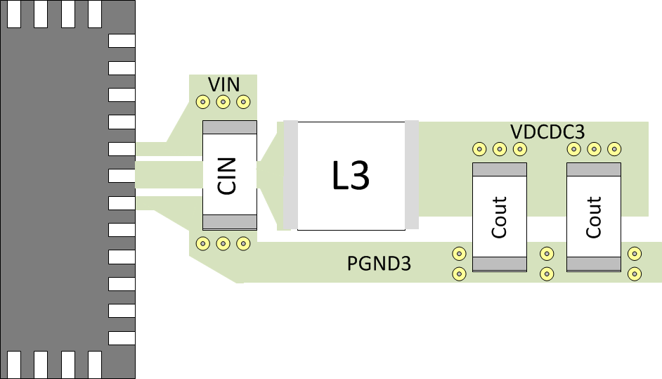 Figure 62. Converter Layout Example