ZHCSH63B October 2017 – January 2020 TLC6C5816-Q1
PRODUCTION DATA.
- 1 特性
- 2 应用
- 3 说明
- 4 修订历史记录
- 5 Pin Configuration and Functions
- 6 Specifications
-
7 Detailed Description
- 7.1 Overview
- 7.2 Functional Block Diagram
- 7.3 Feature Description
- 7.4 Device Functional Modes
- 7.5 Register Maps
- 7.6 Interface Registers
- 8 Application and Implementation
- 9 Power Supply Recommendations
- 10Layout
- 11器件和文档支持
- 12机械、封装和可订购信息
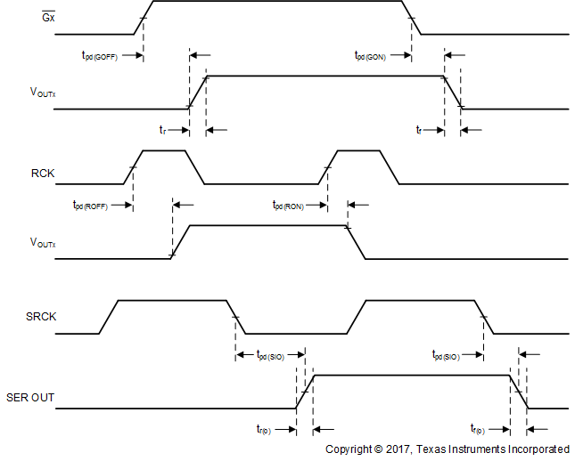
6.7 Switching Characteristics
Vcc = 5 V, TJ = 25ºC, CL = 30 pF, ID = 20 mA unless otherwise specified| PARAMETER | MIN | TYP | MAX | UNIT | |
|---|---|---|---|---|---|
| tpd(deg_open) | LED open to ERR pin pulled down time | 35 | µs | ||
| tpd(deg_short) | LED short to ERR pin pulled down time | 35 | µs | ||
| tpd(GOFF) | Propagation delay time, output off (VOUT equals 10% LED supply voltage) from Gx rising | 250 | ns | ||
| tpd(GON) | Propagation delay time, output on (VOUT equals 90% LED supply voltage) from Gx falling | 250 | ns | ||
| tpd(ROFF) | Propagation delay time, output off (VOUT equals 10% LED supply voltage) from RCK rising | 250 | ns | ||
| tpd(RON) | Propagation delay time, output on (VOUT equals 90% LED supply voltage) from RCK rising | 250 | ns | ||
| tr | Rise time, drain output | 100 | ns | ||
| tf | Fall time, drain output | 100 | ns | ||
| tpd(SIO) | Propagation delay time, SRCK falling edge to SEROUT change | 35 | ns | ||
| tr(o) | SEROUT rise time (10% to 90%) | 20 | ns | ||
| tf(o) | SEROUT fall time (90% to 10%) | 20 | ns | ||
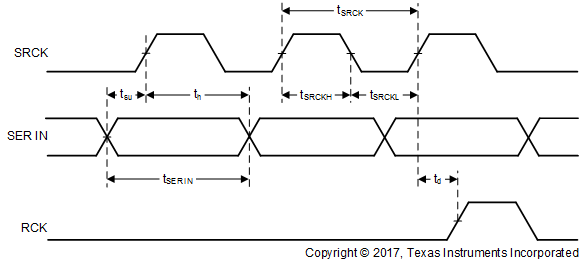
 Figure 1. Timing Diagram of Input Signals
  Figure 2. Timing Diagram of Output Signals