-
适用于汽车系统,具有集成式 ADC 和可调湿性电流的 TIC12400-Q1 24 路输入多开关检测接口 (MSDI)
- 1 特性
- 2 应用
- 3 说明
- 4 Revision History
- 5 Pin Configuration and Functions
- 6 Specifications
- 7 Parameter Measurement Information
-
8 Detailed Description
- 8.1 Overview
- 8.2 Functional Block Diagram
- 8.3
Feature Description
- 8.3.1 VS Pin
- 8.3.2 VDD Pin
- 8.3.3 Device Initialization
- 8.3.4 Device Trigger
- 8.3.5 Device Reset
- 8.3.6 VS Under-Voltage (UV) Condition
- 8.3.7 VS Over-Voltage (OV) Condition
- 8.3.8 Switch Inputs Settings
- 8.3.9 Interrupt Generation and INT Assertion
- 8.3.10 Temperature Monitor
- 8.3.11 Parity Check and Parity Generation
- 8.3.12 Cyclic Redundancy Check (CRC)
- 8.4 Device Functional Modes
- 8.5 Programming
- 8.6 Register Maps
- 8.7 Programming Guidelines
- 9 Application Information Disclaimer
- 10Power Supply Recommendations
- 11Layout
- 12Device and Documentation Support
- 13Mechanical, Packaging, and Orderable Information
- 重要声明
DATA SHEET
适用于汽车系统,具有集成式 ADC 和可调湿性电流的 TIC12400-Q1 24 路输入多开关检测接口 (MSDI)
本资源的原文使用英文撰写。 为方便起见,TI 提供了译文;由于翻译过程中可能使用了自动化工具,TI 不保证译文的准确性。 为确认准确性,请务必访问 ti.com 参考最新的英文版本(控制文档)。
1 特性
- 符合汽车应用要求
- 具有符合 AEC-Q100 标准的下列特性:
- 器件温度等级 1:–40°C 至 125°C 的工作环境温度范围
- 器件 HBM ESD 分类等级 H2
- 器件 CDM ESD 分类等级 C4B
- 提供功能安全
- 旨在支持 12V 汽车系统,并提供过压和欠压警告
- 监控多达 24 路直接开关输入,并可配置其中 10 路输入以监控接地或连接到电池的开关
- 开关输入可承受高达 40V 的电压(负载突降条件)和低至 −24V 的电压(反极性条件)
- 6 种可配置的湿性电流设置:
(0mA、1mA、2mA、5mA、10mA 和 15mA) - 适用于多位模拟开关监控的 10 位集成 ADC
- 适用于数字开关监控并具有 4 个可编程阈值的集成比较器
- 轮询模式下的超低工作电流:
68μA 典型值(tPOLL = 64ms,tPOLL_ACT = 128μs,
全部 24 路输入均有效,比较器模式,所有开关均打开) - 使用 3.3V/5V 串行外设接口 (SPI) 协议直接与 MCU 对接
- 可产生中断来支持所有输入的唤醒操作
- 集成电池和温度传感
- 采用适当的外部组件根据 ISO-10605 在输入引脚上实现 ±8kV 接触放电 ESD 保护
- 38 引脚 TSSOP 封装
3 说明
TIC12400-Q1 是一款先进的多开关检测接口 (MSDI),用于检测 12V 汽车系统中的外部开关状态。TIC12400-Q1 配有集成的 10 位 ADC,用于对多位模拟开关进行监控,并采用比较器以独立于 MCU 的方式对数字开关进行监控。可为 ADC 和比较器设定检测阈值,从而支持各种开关拓扑和系统非理想特性。该器件监控多达 24 路直接开关输入,并可配置其中 10 路输入以监控接地或连接到电池的开关。可为每路输入设定 6 种独特的湿性电流设置,从而支持不同的应用场景。该器件支持所有开关输入的唤醒操作,因此无需持续使 MCU 保持活动状态,进而可降低系统功耗。TIC12400-Q1 还提供集成故障检测、ESD 保护和诊断功能,从而提高系统稳健性。TIC12400-Q1 支持 2 种工作模式:连续模式和轮询模式。连续模式下将连续提供湿性电流。轮询模式下将根据可编程计时器来定期接通湿性电流以对输入状态进行采样,从而显著降低系统功耗。
器件信息
| 器件型号 | 封装(1) | 封装尺寸(标称值) |
|---|---|---|
| TIC12400-Q1 | TSSOP (38) | 9.70mm × 4.40mm |
(1) 如需了解所有可用封装,请参阅数据表末尾的可订购产品附录。
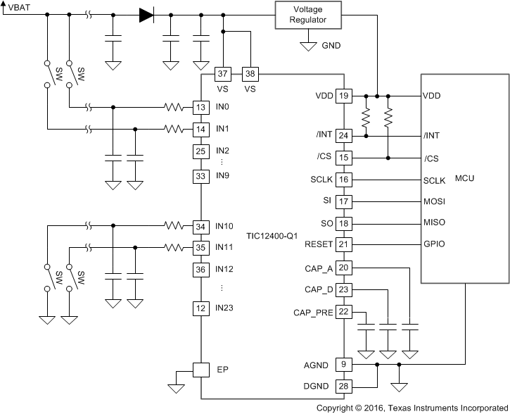
 简化版原理图
4 Revision History
Changes from Revision B (February 2020) to Revision C (February 2022)
Changes from Revision A (September 2017) to Revision B (February 2020)
- Added ADC error for 0 mA current setting in Section 6.5 tableGo
- Added RIN_SC spec for VS above 7 V in Section 6.5 tableGo
- Added RIN_COMP spec for VS above 7 V in Section 6.5 tableGo
- Changed WC_CFG0 for CSO and CSI in matrix mode in Table 8-59 Go
Changes from Revision * (August 2017) to Revision A (September 2017)
- Changed the IWETT value in the Electrical Characteristics tableGo
- Changed From: 4.5 V ≤ VS ≤ 5 V To: 4.5 V ≤ VS < 5.5 V in Figure 6-6 Go
- Changed From: 4.5 V ≤ VS ≤ 35 V To: 5.5 V ≤ VS ≤ 35 V in Figure 6-7 Go
- Changed the Microcontroller Wake-Up section, and Figure 8-9 Go
- Changed Table 9-5 Go
- Changed text in list item 2 From: current ranging between 4.3 mA and 5.6 mA. To: current ranging between 4.5 mA and 5.5 mA (for VS – INX ≥ 3 V condition). Go
5 Pin Configuration and Functions
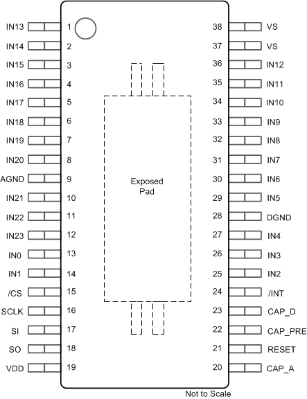
 Figure 5-1 DCP (TSSOP) Package, 38-Pin, Top View
Pin Functions
| PIN | TYPE(1) | DESCRIPTION | |
|---|---|---|---|
| NO. | NAME | ||
| 1 | IN13 | I/O | Ground switch monitoring input with current source. |
| 2 | IN14 | I/O | Ground switch monitoring input with current source. |
| 3 | IN15 | I/O | Ground switch monitoring input with current source. |
| 4 | IN16 | I/O | Ground switch monitoring input with current source. |
| 5 | IN17 | I/O | Ground switch monitoring input with current source. |
| 6 | IN18 | I/O | Ground switch monitoring input with current source. |
| 7 | IN19 | I/O | Ground switch monitoring input with current source. |
| 8 | IN20 | I/O | Ground switch monitoring input with current source. |
| 9 | AGND | P | Ground for analog circuitry. |
| 10 | IN21 | I/O | Ground switch monitoring input with current source. |
| 11 | IN22 | I/O | Ground switch monitoring input with current source. |
| 12 | IN23 | I/O | Ground switch monitoring input with current source. |
| 13 | IN0 | I/O | Ground/VBAT switch monitoring input with configurable current sink or source. |
| 14 | IN1 | I/O | Ground/VBAT switch monitoring input with configurable current sink or source. |
| 15 | CS | I | Active-low input. Chip select from the controller for the SPI Interface. |
| 16 | SCLK | I | Serial clock output from the controller for the SPI Interface. |
| 17 | SI | I | Serial data input for the SPI Interface. |
| 18 | SO | O | Serial data output for the SPI Interface. |
| 19 | VDD | P | 3.3 V to 5.0 V logic supply for the SPI communication. The SPI I/Os are not fail-safe protected: VDD needs to be present during any SPI traffic to avoid excessive leakage currents and corrupted SPI I/O logic levels. |
| 20 | CAP_A | I/O | External capacitor connection for the analog LDO. Use capacitance value of 100 nF. |
| 21 | RESET | I | Keep RESET low for normal operation and drive RESET high and release it to perform a hardware reset of the device. The RESET pin is connected to ground via a 1MΩ pull-down resistor. If not used, the RESET pin shall be grounded to avoid any accidental device reset due to coupled noise onto this pin. |
| 22 | CAP_Pre | I/O | External capacitor connection for the pre-regulator. Use capacitance value of 1 μF. |
| 23 | CAP_D | I/O | External capacitor connection for the digital LDO. Use capacitance value of 100 nF. |
| 24 | INT | O | Open drain output. Pulled low (internally) upon change of state on the input or occurrence of a special event. |
| 25 | IN2 | I/O | Ground/VBAT switch monitoring input with configurable current sink or source. |
| 26 | IN3 | I/O | Ground/VBAT switch monitoring input with configurable current sink or source. |
| 27 | IN4 | I/O | Ground/VBAT switch monitoring input with configurable current sink or source. |
| 28 | DGND | P | Ground for digital circuitry. |
| 29 | IN5 | I/O | Ground/VBAT switch monitoring input with configurable current sink or source. |
| 30 | IN6 | I/O | Ground/VBAT switch monitoring input with configurable current sink or source. |
| 31 | IN7 | I/O | Ground/VBAT switch monitoring input with configurable current sink or source. |
| 32 | IN8 | I/O | Ground/VBAT switch monitoring input with configurable current sink or source. |
| 33 | IN9 | I/O | Ground/VBAT switch monitoring input with configurable current sink or source. |
| 34 | IN10 | I/O | Ground switch monitoring input with current source. |
| 35 | IN11 | I/O | Ground switch monitoring input with current source. |
| 36 | IN12 | I/O | Ground switch monitoring input with current source. |
| 37 | VS | P | Power supply input pin. |
| 38 | VS | P | Power supply input pin. |
| --- | EP | P | Exposed Pad. The exposed pad is not electrically connected to AGND or DGND. Connect EP to the board ground to achieve rated thermal and ESD performance. |
(1) I = input, O = output, I/O = input and output, P = power.
6 Specifications
6.1 Absolute Maximum Ratings
Over operating free-air temperature range (unless otherwise noted).(1)
| MIN | MAX | UNIT | ||
|---|---|---|---|---|
| Input voltage | VS, INT | -0.3 | 40(2) | V |
| VDD, SCLK, SI, SO, CS, RESET | -0.3 | 6 | V | |
| IN0- IN23 | -24 | 40(2) | V | |
| CAP_Pre | -0.3 | 5.5 | V | |
| CAP_A | -0.3 | 5.5 | V | |
| CAP_D | -0.3 | 2 | V | |
| Operating junction temperature, TJ | -40 | 150 | °C | |
| Storage temperature, Tstg | -55 | 155 | °C | |
(1) Stresses beyond those listed under Absolute Maximum Ratings may cause permanent damage to the device. These are stress ratings only, which do not imply functional operation of the device at these or any other conditions beyond those indicated under Recommended Operating Conditions. Exposure to absolute-maximum-rated conditions for extended periods may affect device reliability.
(2) Tested for load dump and jump start conditions with nominal operating voltage no greater than 16 V for the life of a 12-V automotive system. Refer to Section 9.2 for more details.
6.2 ESD Ratings
| VALUE | UNIT | ||||
|---|---|---|---|---|---|
| V(ESD) | Electrostatic discharge | Human-body model (HBM), per AEC Q100-002(1) | All pins | ±2000 | V |
| Pins IN0-IN23(2) | ±4000 | ||||
| Charged-device model (CDM), per AEC Q100-011 | All pins | ±500 | |||
| Corner pins (pin 1, 19, 20 and 38) | ±750 | ||||
Contact discharge, un-powered, per ISO- 10605:
|
Pins IN0-IN23 | ±8000 | |||
Contact discharge, powered-up, per ISO- 10605:
|
Pins IN0-IN23 | ±8000 | |||
(1) AEC Q100-002 indicates that HBM stressing shall be in accordance with the ANSI/ESDA/JEDEC JS-001 specification.
(2) ±4-kV rating on pins IN0-IN23 are stressed with respect to GND (with AGND, DGND, and EP tied together).
6.3 Recommended Operating Conditions
Over operating free-air temperature range and VS = 12 V (unless
otherwise noted).
| MIN | NOM | MAX | UNIT | |||
|---|---|---|---|---|---|---|
| VS | Power supply voltage | 4.5 | 35 (2) | V | ||
| VDD | Logic supply voltage | 3.0 | 5.5 | V | ||
| V/INT | INT pin voltage | 0 | 35(2) | V | ||
| VINX | IN0 to IN23 input voltage | 0 | 35(2) | V | ||
| VRESET | RESET pin voltage | 0 | 5.5 | V | ||
| VSPI_IO | SPI input/output logic level | 0 | VDD | V | ||
| fSPI | SPI communication frequency | 20(1) | 4M | Hz | ||
| TA | Operating free-air temperature | -40 | 125 | °C | ||
(1) Lowest frequency characterized.
(2) Tested for load dump and jump start conditions with nominal operating voltage no greater than 16-V for the life of a 12-V automotive system. Refer to Section 9.2 for more details.