-
TLV62569 采用 SOT 封装的 2A 高效同步降压转换器
- 1 特性
- 2 应用
- 3 说明
- 4 修订历史记录
- 5 Pin Configuration and Functions
- 6 Specifications
- 7 Detailed Description
- 8 Application and Implementation
- 9 Power Supply Recommendations
- 10Layout
- 11器件和文档支持
- 12机械、封装和可订购信息
- 重要声明
TLV62569 采用 SOT 封装的 2A 高效同步降压转换器
1 特性
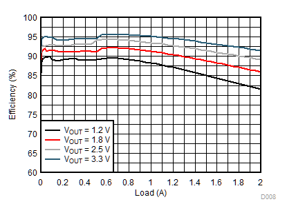
- 效率高达 95%
- 低 RDS(ON),可在 100mΩ 和 60mΩ 之间切换
- 输入电压范围:2.5V 至 5.5V
- 可调输出电压:0.6V 至 VIN
- 针对轻载效率的省电模式
- 针对最低压降的 100% 占空比
- 35µA 静态工作电流
- 1.5MHz 典型开关频率
- 电源正常输出
- 过流保护
- 内部软启动
- 热关断保护
- 采用小外形尺寸晶体管 (SOT) 封装
- 与 TLV62568 引脚兼容
- 使用 TLV62569 并借助 WEBENCH® Power Designer 创建定制设计方案
2 应用
- 通用负载点 (POL) 电源
- 机顶盒
- 网络视频摄像头
- 无线路由器
- 硬盘
3 说明
TLV62569 器件是一款同步降压 DC-DC 转换器,专门针对高效和紧凑型解决方案进行了优化。该器件集成的开关能够提供高达 2A 的输出电流。
在中等负载或重载条件下,该器件运行在脉宽调制 (PWM) 模式下,开关频率为 1.5MHz。在轻载情况下,该器件自动进入节能模式 (PSM),从而在整个负载电流范围内保持高效率。关断时,流耗减少至 2μA 以下。
TLV62569 的输出电压可通过一个外部电阻分压器进行调节。内部软启动电路可限制启动期间的浪涌电流。此外, 还内置了 诸如输出过流保护、热关断保护和电源正常输出等其他特性。该器件提供 SOT23 和 SOT563 两种封装。
器件信息(1)
| 器件型号 | 封装 | 封装尺寸(标称值) |
|---|---|---|
| TLV62569DBV | SOT23 (5) | 2.90mm x 2.80mm |
| TLV62569PDDC | SOT23 (6) | |
| TLV62569DRL | SOT563 (6) | 1.60mm x 1.60mm |
| TLV62569PDRL | SOT563 (6) |
- 要了解所有可用封装,请参阅数据表末尾的可订购产品附录。
Device Images
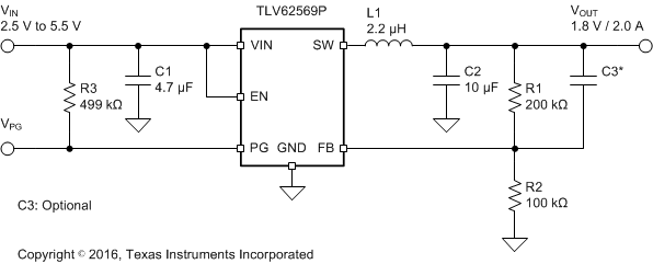
简化电路原理图
5V 输入电压下的效率
4 修订历史记录
Changes from B Revision (July 2017) to C Revision
- Changed TLV62569DRL 和 TLV62569PDRL 更改为生产状态。Go
- Added 在器件比较表中添加了 TLV62569DRL 和 TLV62569PDRL 的标记符号Go
- Added DRL package thermal information Go
- Corrected editorial error of EN pin threshold voltageGo
- Added current limit for TLV62569DRL and TLV62569PDRL Go
- Added TLV62569PDRL layout exampleGo
Changes from A Revision (March 2017) to B Revision
- Changed TLV62569PDDC 更改为生产状态Go
- 器件比较表移至第 1 页Go
- Added DDC package thermal informationGo
- Added startup time of TLV62569PDDCGo
Changes from * Revision (December 2016) to A Revision
- Added WEBENCH® 模型 Go
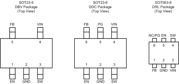
5 Pin Configuration and Functions
Pin Functions
| PIN NUMBER | I/O/PWR | DESCRIPTION | |||
|---|---|---|---|---|---|
| NAME | SOT23-5 | SOT23-6 | SOT563-6 | ||
| EN | 1 | 1 | 5 | I | Device enable logic input. Logic high enables the device, logic low disables the device and turns it into shutdown. Do not leave floating. |
| GND | 2 | 2 | 2 | PWR | Ground pin. |
| SW | 3 | 3 | 4 | PWR | Switch pin connected to the internal FET switches and inductor terminal. Connect the inductor of the output filter to this pin. |
| VIN | 4 | 4 | 3 | PWR | Power supply voltage input. |
| PG | - | 5 | 6 | O | Power good open drain output pin for TLV62569P. The pull-up resistor should not be connected to any voltage higher than 5.5V. If it's not used, leave the pin floating. |
| FB | 5 | 6 | 1 | I | Feedback pin for the internal control loop. Connect this pin to an external feedback divider. |
| NC | - | - | 6 | O | No connection pin for TLV62569DRL. The pin can be connected to the output or the ground. Or leave it floating. |
6 Specifications
6.1 Absolute Maximum Ratings
Over operating temperature range (unless otherwise noted)(1)| MIN | MAX | UNIT | ||
|---|---|---|---|---|
| Voltage(2) | VIN, EN, PG | –0.3 | 6 | V |
| SW (DC) | –0.3 | VIN+0.3 | V | |
| SW (AC, less than 10ns)(3) | –3.0 | 9 | V | |
| FB | –0.3 | 5.5 | V | |
| Operating junction temperature, TJ | –40 | 150 | °C | |
| Storage temperature, Tstg | –65 | 150 | °C | |
6.2 ESD Ratings
| VALUE | UNIT | |||
|---|---|---|---|---|
| V(ESD) | Electrostatic discharge | Human-body model (HBM), per ANSI/ESDA/JEDEC JS-001(1) | ±2000 | V |
| Charged-device model (CDM), per JEDEC specification JESD22-C101(2) | ±500 | V | ||
6.3 Recommended Operating Conditions(1)
| MIN | TYP | MAX | UNIT | ||
|---|---|---|---|---|---|
| VIN | Input voltage | 2.5 | 5.5 | V | |
| VOUT | Output voltage | 0.6 | VIN | V | |
| IOUT | Output current | 0 | 2 | A | |
| TJ | Operating junction temperature | –40 | 125 | °C | |
| ISINK_PG | Sink current at PG pin | 1 | mA |
6.4 Thermal Information
| THERMAL METRIC(1) | DBV (5 Pins) | DDC (6 Pins) | DRL (6 Pins) | UNIT | |
|---|---|---|---|---|---|
| RθJA | Junction-to-ambient thermal resistance | 188.2 | 106.2 | 146.3 | °C/W |
| RθJC(top) | Junction-to-case (top) thermal resistance | 137.5 | 52.9 | 51.0 | °C/W |
| RθJB | Junction-to-board thermal resistance | 41.2 | 31.2 | 27.0 | °C/W |
| ψJT | Junction-to-top characterization parameter | 31.4 | 11.3 | 2.2 | °C/W |
| ψJB | Junction-to-board characterization parameter | 40.6 | 31.6 | 27.6 | °C/W |
| RθJC(bot) | Junction-to-case (bottom) thermal resistance | n/a | n/a | n/a | °C/W |
6.5 Electrical Characteristics
VIN = 5.0 V, TJ = 25°C, unless otherwise noted6.6 Typical Characteristics
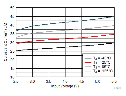
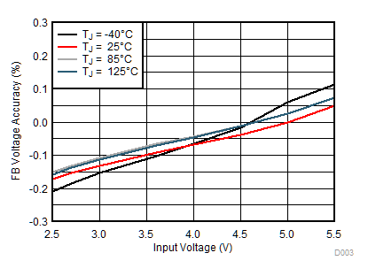
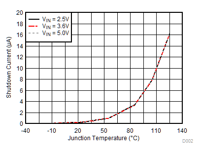
7 Detailed Description
7.1 Overview
The TLV62569 is a high-efficiency synchronous step-down converter. The device operates with an adaptive off time with peak current control scheme. The device operates at typically 1.5-MHz frequency pulse width modulation (PWM) at moderate to heavy load currents. Based on the VIN/VOUT ratio, a simple circuit sets the required off time for the low-side MOSFET. It makes the switching frequency relatively constant regardless of the variation of input voltage, output voltage, and load current.
7.2 Functional Block Diagrams
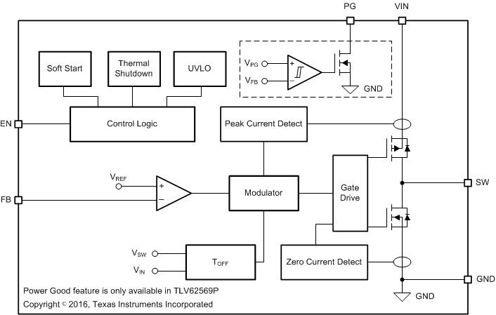 Figure 4. TLV62569 Functional Block Diagram
7.3 Feature Description
7.3.1 Power Save Mode
The device automatically enters Power Save Mode to improve efficiency at light load when the inductor current becomes discontinuous. In Power Save Mode, the converter reduces switching frequency and minimizes current consumption. In Power Save Mode, the output voltage rises slightly above the nominal output voltage. This effect is minimized by increasing the output capacitor.
7.3.2 100% Duty Cycle Low Dropout Operation
The device offers a low input-to-output voltage differential by entering 100% duty cycle mode. In this mode, the high-side MOSFET switch is constantly turned on and the low-side MOSFET is switched off. The minimum input voltage to maintain output regulation, depending on the load current and output voltage, is calculated as:
where
- RDS(ON) = High side FET on-resistance
- RL = Inductor ohmic resistance (DCR)
7.3.3 Soft Startup
After enabling the device, internal soft startup circuitry ramps up the output voltage which reaches nominal output voltage during a startup time. This avoids excessive inrush current and creates a smooth output voltage rise slope. It also prevents excessive voltage drops of primary cells and rechargeable batteries with high internal impedance.
The TLV62569 is able to start into a pre-biased output capacitor. The converter starts with the applied bias voltage and ramps the output voltage to its nominal value.
7.3.4 Switch Current Limit
The switch current limit prevents the device from high inductor current and drawing excessive current from a battery or input voltage rail. Excessive current might occur with a heavy load or shorted output circuit condition. The TLV62569 adopts the peak current control by sensing the current of the high-side switch. Once the high-side switch current limit is reached, the high-side switch is turned off and low-side switch is turned on to ramp down the inductor current with an adaptive off-time.
7.3.5 Under Voltage Lockout
To avoid mis-operation of the device at low input voltages, under voltage lockout is implemented that shuts down the device at voltages lower than VUVLO with VHYS_UVLO hysteresis.