-
LP5560 具有单线制接口的可编程 LED 驱动器
- 1 特性
- 2 应用
- 3 说明
- 4 修订历史记录
- 5 Pin Configuration and Functions
- 6 Specifications
-
7 Detailed Description
- 7.1 Overview
- 7.2 Functional Block Diagram
- 7.3 Feature Description
- 7.4 Device Functional Modes
- 7.5 Programming
- 7.6 Registers
- 8 Application and Implementation
- 9 Power Supply Recommendations
- 10Layout
- 11器件和文档支持
- 12机械、封装和可订购信息
- 重要声明
LP5560 具有单线制接口的可编程 LED 驱动器
1 特性
- 宽输入电压范围:2.7V 至 5.5V
- 可调节输出电流:2.8mA 至 19.5mA
- 具有电流上升及下降时间控制的可编程闪烁序列
- 用于无编程功能的简易系统的默认闪烁序列
- 单线制接口
- 恒流高侧输出驱动器
- 极低的余量电压(典型值为 40mV)
- 超小解决方案尺寸 - 无外部组件
2 应用
- 手机及其他便携式设备的 LED 指示灯
- 读卡器
- 加油机
- 计步器
- 电子门禁控制
- 需要简单反馈的设备
3 说明
LP5560 是一款可编程的 LED 驱动器,能够生成各种闪烁序列,每个序列最多由 3 个不同长度的脉冲组成。可以通过单线制接口对闪烁序列进行编程。可编程参数包括导通和关断时间,以及上升和下降时间。LP5560 内置默认序列,能够应用于无编程功能的简易系统中。
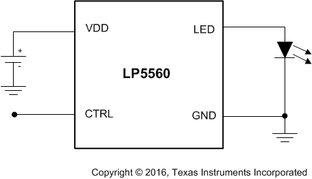
该器件具有超低余量电压,无需使用升压放大器。指示灯 LED 可以由电池直接驱动。该器件采用小型封装,并且无需任何外部组件,最大限度地减小了解决方案的尺寸。
LP5560 采用间距为 0.4mm 的 TI 微型 4 引脚 DSBGA 封装。
器件信息(1)
| 器件型号 | 封装 | 封装尺寸(标称值) |
|---|---|---|
| LP5560 | DSBGA (4) | 0.886mm x 0.886mm |
- 要了解所有可用封装,请见数据表末尾的可订购产品附录。
典型应用
4 修订历史记录
Changes from C Revision (May 2013) to D Revision
- Added 其他应用,器件信息和引脚配置和功能部分,ESD 额定值和热性能信息表,特性 描述,器件功能模式,应用和实施,电源相关建议,布局,器件和文档支持以及机械、封装和可订购信息部分Go
- Changed RθJA value from "120°C/W" to "184.3°C/W"; added additional thermal valuesGo
Changes from B Revision (April 2013) to C Revision
- Changed layout of National Data Sheet to TI formatGo
5 Pin Configuration and Functions

Pin Functions
| PIN | TYPE(1) | DESCRIPTION | |
|---|---|---|---|
| NO. | NAME | ||
| A1 | VDD | P | Power supply pin |
| A2 | LED | A | Current source output |
| B1 | GND | G | Ground |
| B2 | CTRL | DI | Single-wire interface input |
6 Specifications
6.1 Absolute Maximum Ratings
over operating free-air temperature range (unless otherwise noted)(1)(2)(3)| MIN | MAX | UNIT | ||
|---|---|---|---|---|
| Voltage on VDD pin | −0.3 | 6 | V | |
| Voltage on other pins (CTRL,LED)(4) | −0.3 | VDD + 0.3 V with 6 V maximum | V | |
| Continuous power dissipation(5) | Internally Limited | |||
| Junction temperature, TJ-MAX | 125 | °C | ||
| Storage temperature, Tstg | −65 | 150 | °C | |
6.2 ESD Ratings
| VALUE | UNIT | |||
|---|---|---|---|---|
| V(ESD) | Electrostatic discharge | Human-body model (HBM), per ANSI/ESDA/JEDEC JS-001(1) | ±2000 | V |
| Charged-device model (CDM), per JEDEC specification JESD22-C101(2) | ±1000 | |||
6.3 Recommended Operating Conditions
over operating free-air temperature range (unless otherwise noted)(1)(2)| MIN | NOM | MAX | UNIT | ||
|---|---|---|---|---|---|
| Voltage on power pin (VDD) | 2.7 | 5.5 | V | ||
| Junction temperature, TJ | −30 | 125 | °C | ||
| Ambient temperature, TA(1) | −30 | 85 | °C | ||
6.4 Thermal Information
| THERMAL METRIC(1) | LP5560 | UNIT | |
|---|---|---|---|
| YFQ (DSBGA) | |||
| 4 PINS | |||
| RθJA | Junction-to-ambient thermal resistance | 184.3 | °C/W |
| RθJC(top) | Junction-to-case (top) thermal resistance | 1.8 | °C/W |
| RθJB | Junction-to-board thermal resistance | 103.2 | °C/W |
| ψJT | Junction-to-top characterization parameter | 9.1 | °C/W |
| ψJB | Junction-to-board characterization parameter | 103.1 | °C/W |
6.5 Electrical Characteristics
Unless otherwise specified: VIN = 3.6 V, CTRL = 3.6 V, VLED = 3.1 V; typical limits are for TA = 25°C, and minimum and maximum limits apply over the operating ambient temperature range (−30°C < TA < +85°C).(1)(2)| PARAMETER | TEST CONDITIONS | MIN | TYP | MAX | UNIT | |
|---|---|---|---|---|---|---|
| ISD | Shutdown supply current | CTRL = 0 V | 0.4 | 0.75 | µA | |
| IQ | Quiescent supply current | ILED = 0 mA | 25 | 30 | ||
| ILED | LED output current | ISET = 0 | 2.26 | 2.8 | 3.34 | mA |
| ISET = 1 (default) | 4.61 | 5.3 | 5.99 | |||
| ISET = 2 | 6.78 | 7.8 | 8.82 | |||
| ISET = 3 | 8.87 | 10.2 | 11.53 | |||
| ISET = 4 | 10.96 | 12.6 | 14.24 | |||
| ISET = 5 | 13.5 | 15.0 | 16.5 | |||
| ISET = 6 | 15.05 | 17.3 | 19.55 | |||
| ISET = 7 | 16.96 | 19.5 | 22.04 | |||
| ΔILED%/ΔVIN | Line regulation | 2.7 V ≤ VIN ≤ 4.5 V | –3% | 3% | %/1V | |
| IDX = 5.3 mA, Vƒ = 2.5 V | ||||||
| ΔILED%/ΔVLED(3) | Load regulation | 1.7 V ≤ VLED ≤ 3.4 V, ILED = 5.3 mA | 0.6 | |||
| VHR | Headroom voltage(4) | ILED = 5.3 mA | 40 | 100 | mV | |
| ILED = 19.5 mA | 40 | |||||
| VIH | Logic input high level | VIN = 2.7 V to 5.5 V | 1.1 | V | ||
| VIL | Logic input low level | VIN = 2.7 V to 5.5 V | 0.6 | V | ||
| ICTRL | CTRL pin leakage current | CTRL = 1.8 V | 400 | nA | ||
| T_cycle_H | LED On time | Adjustable(5), TA = 25°C | 13.2 | 3009.6 | ms | |
| T_cycle_L | LED OFF time | 26.4 | 6019.2 | ms | ||
| Trise | LED current rise time(6) | 0 | 1584 | ms | ||
| Tfall | LED current fall time(6) | 0 | 1584 | ms | ||
| Fade resolution | Rise/fall time resolution | See(5) | 105.6 | ms | ||
6.6 Single-Wire Interface Timing Requirements
See (1)(2) and Figure 1| MIN | MAX | UNIT | ||
|---|---|---|---|---|
| TC_ON | Command pulse on time | 15 | µs | |
| TC_OFF | Command pulse off time | 30 | µs | |
| TT_ON | Minimum training pulse on time(3) | 200 | µs | |
| TT_OFF | Minimum training pulse off time(4) | 200 | µs | |
| TCAL | Calibration pulse length | 0.35 | 8 | ms |
| T ENTER | Command entering period | 500 | µs | |
| T ENTER+T BLANK | Command entering period + Blank period | 1500 | µs | |
 Figure 1. Interface Timing
6.7 Typical Characteristics
TJ = 25°C. Unless otherwise noted, typical characteristics apply to the Functional Block Diagram with: VIN = 3.6 V, RISET = 24 kΩ, CIN = 100 nF.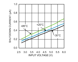
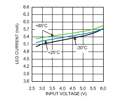
| 5 mA |
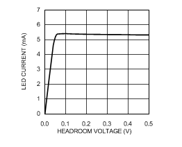
| 5 mA |
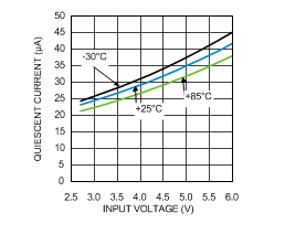
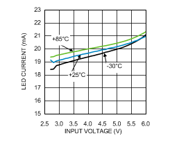
| 20 mA |
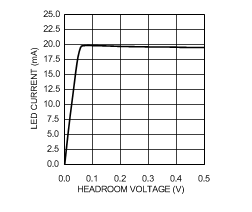
| 20 mA |
7 Detailed Description
7.1 Overview
The LP5560 is a programmable LED driver with a single-wire interface. It is designed to drive a single indicator LED with different blinking sequences. Up to three pulses with different on and off times can be programmed into the device. LED current rise and fall times can also be independently controlled. Blinking sequence is stored into volatile memory, thus removing input voltage VIN resets the memory into default state.
The high-side LED driver has very low headroom voltage requirement and can drive most indicator LEDs directly from battery voltage. A single CTRL pin is used to control the device on and off and to change settings of the device. A default blinking sequence is programmed into the LP5560 to enable use of the devices in simply applications without programming capabilities.
7.2 Functional Block Diagram
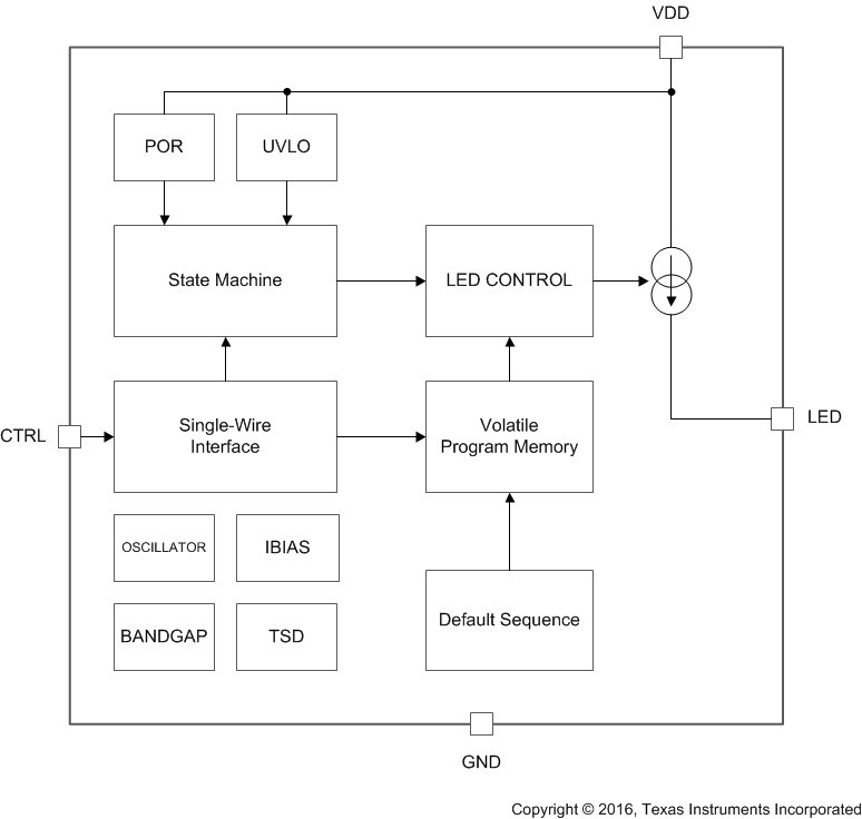
7.3 Feature Description
7.3.1 LED Driver Headroom Voltage
The current source is connected internally between the VDD and LED output pins. The voltage across the current source, (VVDD − VLED), is referred as headroom voltage (VHR). The current source requires a sufficient amount of headroom voltage to be present across it in order to regulate the output current properly. The LP5560 headroom voltage requirement is 40 mV (typical) and does not depend on the current setting.
7.3.2 Single-Wire Interface
The LP5560 has one digital control input (CTRL). Threshold levels of CTRL input are fixed to support control from low-voltage controller. The CTRL signal is used to control the mode of the circuit. The rising edge of the CTRL signal activates the circuit and starts a command entering period. During the command entering period all rising edges are counted. After command entering period there is a blank period when no rising edges are allowed. If there are any rising edges during blank period these are not detected. User must take care not to start the training sequence before blank period has elapsed or the training sequence is corrupted.
If CTRL is left high after command entering period, the consequent command is performed right after the blank period. In case of run once command CTRL pin can be set low after the command entering period and execution of the command starts once CTRL pin is pulled high after blank period.
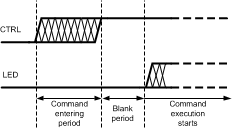 Figure 8. Single-Wire Interface
The LP5560 has four different commands. Command depends on the number of rising edges during command entering period. If there are more than 4 rising edges during command entering period command is ignored. Note that even in this case blank period needs to elapse before next command can be given.
Table 1. LP5560 Commands
| COMMAND | NUMBER OF RISING EDGES DURING COMMAND ENTERING PERIOD |
|---|---|
| Run | 1 |
| Training start | 2 |
| Training end | 3 |
| Run once | 4 |
7.3.2.1 Run Command
One rising edge of the CTRL signal within command entering period is interpreted as a run command. The CTRL pin must be kept high during blank period. If the CTRL pin is pulled low during command entering period or blank period device goes to stand by. In run mode (mode bit = 1) blinking sequence is started right after Blank period and it is repeated as long as CTRL signal is kept high. When the CTRL signal is set low device goes into standby mode (Figure 9).
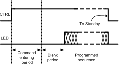 Figure 9. Run Mode
In follow mode (mode bit = 0) LED is turned on right after a blank period, and it stays on as long as CTRL is kept high. When CTRL signal is set low LED is turned off and device goes into standby mode (Figure 10).
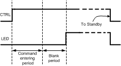 Figure 10. Follow Mode
7.3.2.2 Training Start Command
Two rising edges of CTRL signal within command entering period is interpreted as training start command. Training start command starts training sequence. Different blinking sequences can be trained into device in training mode. Training mode is described in more details in Training Mode.
7.3.2.3 Training End Command
Three rising edges of CTRL signal within command entering period is interpreted as training end command. Training end is used to stop the training sequence.
7.3.2.4 Run-Once Command
Four rising edges of the CTRL signal within command entering period is interpreted as a run-once command. Programmed blinking sequence is performed once after a run-once command. If CTRL is kept high after command entering period the programmed blinking sequence starts right after the blank period has elapsed (Figure 11). The CTRL signal must stay high as long as programmed blinking sequence is executed. If CTRL is set low during execution of blinking sequence, device goes to standby and execution of blinking sequence is stopped.
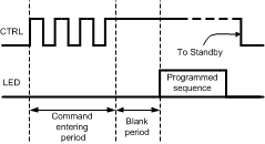 Figure 11. Run-Once Command
If CTRL signal is low after command entering period, blinking sequence is executed once the CTRL is set high (Figure 12).
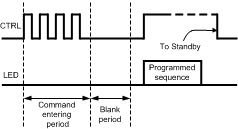 Figure 12. Delayed Run-Once Command
If device is in follow mode (mode bit is 0) the run-once command turns the LED on, and it is kept on as long as CTRL is held high.
7.3.3 Training Mode
Figure 17 shows an example of a full training sequence with three pulses. Training mode starts with a training start command. Training start command is followed by blank time during which no rising edges are allowed. Blank time is followed by calibration pulse. Calibration pulse length (TCAL) defines the speed of the training sequence and can vary from 350 µs to 8 ms. During parameter settings register values are incremented at speed defined by TCAL. For example, if calibration pulse length is 1 ms and current setting pulse length is 3.3 ms, the current-setting value is 3 (current-set register is incremented 3 times). If the parameter-setting pulse is shorter than the calibration pulse, then the corresponding parameter is set to 0.
The next rising edge after calibration pulse starts LED driver current setting (I). LED driver current is recorded once CTRL is pulled low. Note that there are empty low times before and after current setting pulse. For the following pulses both CTRL high and CTRL low times are used to set the parameters. Next the CTRL high time defines the LED current rise time setting for pulse 1 (R1). When R1 setting is started mode bit is set to 0. This sets the LP5560 device into follow mode. Mode bit is set to 1 after first off time has been saved into register. This means that at least one full pulse must be trained into memory to set the device into run mode.
CTRL low time after R1 defines the LED on time for pulse 1 (ON1). CTRL high time after ON1 sets the LED current fall time (F1). CTRL low time after F1 sets pulse 1 off time (OFF1). Once rising edge of CTRL is detected after first off time setting mode bit is set to 1 (run mode) and the number of pulses register (NOP[1:0]) is set to 1. This indicates that one full pulse has been trained into memory.
Rise, on, fall, and off times for pulse 2 and 3 are set the same way as for pulse 1. Note that NOP register is always incremented after OFFx time setting. This means that all pulse parameters (rise, on, fall, and off times) must be trained for each pulse make it valid. The training sequence is ended with training end command.
7.3.3.1 Ending the Training Sequence
A training end command can be given at any time of the training sequence except during blank time. Outcome of the training sequence depends on the place of the training end command. If a training end command is given after any of the off-time setting (OFF1, OFF2 or OFF3), mode bit is set to 1, and the corresponding number of pulses are stored into memory. If a training end command is given after any of the other pulse parameters (Rx, ONx or Fx) that pulse is ignored. For example, if training end command is given after ON2 pulse 2 is ignored and blinking sequence includes only pulse 1.
7.3.3.2 Reset to Default
If a training end command is given right after a training start command, the LP5560 is reset back to factory defaults (Figure 13). In this case the mode bit is set to 1 (run mode) with the factory-set default blinking sequence.
 Figure 13. Reset to Default
7.3.3.3 Changing the LED Current
The LP5560 devices allows changing the LED output current without the need to reprogram the previously programmed blinking sequence. This is done by giving the training end command after current setting (Figure 14). In this case only the current setting changes. If a blinking sequence was programmed into the LP5560 device it remains unchanged. If mode bit was 0 (follow mode) before the training sequence it remains 0.
 Figure 14. Current Programming Sequence
7.3.3.4 Entering Follow Mode
Mode bit can be set to 0 (follow mode) in two ways. If training end command is given after calibration pulse mode bit is set to 0 (follow mode) and the previously set LED output current setting remains unchanged (Figure 15).
 Figure 15. Entering Follow Mode
If training end command is given after R1, ON1 or F1 mode bit is set to 0 (follow mode) and new current setting is stored to current register (Figure 16). If a training end command is given after F1 CTRL low time before training end command needs to be less than minimum training pulse off time (200 µs). Otherwise off time OFF1 is set to minimum value, and pulse 1 is stored into memory.
 Figure 16. Entering Follow Mode With New Current Setting
7.3.3.5 Timeout
If during training CTRL stays constant for more than 127 × TCAL time this is interpreted as timeout. For example, if calibration pulse length TCAL is 1 ms, timeout time is 127 ms. Timeout ends the training sequence. Timeout is considered as a false training, and it is a good practice to always give a complete training sequence after timeout to ensure correct data is stored into memory.
 Figure 17. Full Training Sequence
7.3.4 LED Output Current Setting
The LED output current can be set from 2.8 mA to 19.5 mA in 7 steps. Duration of the current setting pulse (I) defines the current setting.
Table 2. LED Current Setting
| CURRENT SETTING | LED CURRENT (mA) |
|---|---|
| 0 | 2.8 |
| 1 | 5.3 default |
| 2 | 7.8 |
| 3 | 10.2 |
| 4 | 12.6 |
| 5 | 15.0 |
| 6 | 17.3 |
| 7 | 19.5 |
7.3.5 Rise and Fall Time Settings
Rise and fall times of each pulse can be programmed independently. Rise and fall time can be set from 0 to 1584 ms with 105.6 ms steps. Rise and fall times are generated using a combined PWM and current control. Ramp has 32 PWM steps. For the first 8 steps LED current is decreased to 12.5%. For the remaining steps current is set to 100%. Each step is 3.3 ms long. This results in the minimum ramp time of 3.3 ms × 32 = 105.6 ms. When ramp time is increased each PWM step is done multiple times. When setting rise and fall times they are always rounded down. For example if calibration pulse length is 1 ms and rise time setting pulse is 2.9 ms rise time is set to 2 which is 211.2 ms. Rise and fall times can be set to zero by giving pulse that is shorter than calibration pulse.
Table 3. Rise and Fall Time Settings
| RAMP SETTING | RAMP TIME (ms) |
|---|---|
| 0 | 0 |
| 1 | 105.6 |
| 2 | 211.2 |
| 3 | 316.8 |
| 4 | 422.4 |
| 5 | 528 default |
| 6 | 633.6 |
| 7 | 739.2 |
| 8 | 844.8 |
| 9 | 950.4 |
| 10 | 1056 |
| 11 | 1161.6 |
| 12 | 1267.2 |
| 13 | 1372.8 |
| 14 | 1478.4 |
| 15 | 1584 |
7.3.6 LED ON-Time Setting
LED on time has 5-bit control. On time can be controlled from 13.2 ms to 3009.6 ms in 31 steps. Step size is not constant to increase resolution on shorter ON times. With longer on times also the step size is increased. Table 4 shows the available on times.
Table 4. LED ON-Time Setting
| SETTING | LED ON TIME (ms) |
|---|---|
| 0 | 13.2 |
| 1 | 26.4 |
| 2 | 52.8 |
| 3 | 105.6 |
| 4 | 158.4 |
| 5 | 211.2 |
| 6 | 264 |
| 7 | 316.8 |
| 8 | 369.6 |
| 9 | 435.6 |
| 10 | 501.6 default |
| 11 | 594 |
| 12 | 699.6 |
| 13 | 805.2 |
| 14 | 910.8 |
| 15 | 1016.4 |
| 16 | 1122 |
| 17 | 1227.6 |
| 18 | 1353 |
| 19 | 1478.4 |
| 20 | 1603.8 |
| 21 | 1729.2 |
| 22 | 1854.6 |
| 23 | 1980 |
| 24 | 2105.4 |
| 25 | 2230.8 |
| 26 | 2356.2 |
| 27 | 2481.6 |
| 28 | 2613.6 |
| 29 | 2745.6 |
| 30 | 2877.6 |
| 31 | 3009.6 |
7.3.7 LED OFF-Time Setting
LED off time has also 5-bit control. Off time can be controlled from 26.4 ms to 6019.2 ms in 31 steps. Off time is always twice as long as on time with same setting.
Table 5. LED OFF-Time Setting
| SETTING | LED OFF TIME (ms) |
|---|---|
| 0 | 26.4 |
| 1 | 52.8 |
| 2 | 105.6 |
| 3 | 211.2 |
| 4 | 316.8 |
| 5 | 422.4 |
| 6 | 528 |
| 7 | 633.6 |
| 8 | 739.2 |
| 9 | 871.2 |
| 10 | 1003.2 |
| 11 | 1188 |
| 12 | 1399.2 |
| 13 | 1610.4 default |
| 14 | 1821.6 |
| 15 | 2032.8 |
| 16 | 2244 |
| 17 | 2455.2 |
| 18 | 2706 |
| 19 | 2956.8 |
| 20 | 3207.6 |
| 21 | 3458.4 |
| 22 | 3709.2 |
| 23 | 3960 |
| 24 | 4210.8 |
| 25 | 4461.6 |
| 26 | 4712.4 |
| 27 | 4963.2 |
| 28 | 5227.2 |
| 29 | 5491.2 |
| 30 | 5755.2 |
| 31 | 6019.2 |
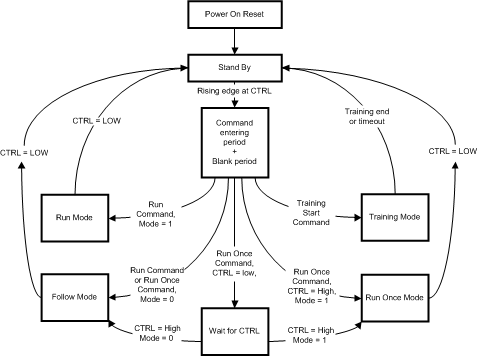
7.4 Device Functional Modes
-
POWER-ON RESET When input voltage is applied to VDD pin device goes through power on reset (POR). During POR defaults are set into control registers.
-
STANDBY: After POR device goes to standby. This is the low power mode when all the internal blocks are shut down.
-
COMMAND ENTERING PERIOD + BLANK PERIOD: Rising edge of the CTRL signal activates the circuit and starts a command entering period. During the command entering period all rising edges are counted. After command entering period there is a blank period when no rising edges are allowed.
-
RUN: If mode bit is 1 (run mode) and run command has been detected device goes into run mode. In run mode LP5560 generates the programmed blinking sequence.
-
FOLLOW MODE: If mode bit is 0 (follow mode) and run command or run once command has been detected LP5560 goes into follow mode. In follow mode LED stays on as long as CTRL pin is held high.
-
RUN-ONCE MODE: If run once command has been detected and mode bit is 1 (run mode) device goes into run-once mode. In run-once mode LP5560 generates the programmed blinking sequence once. CTRL must be high as long as blinking sequence is running.
-
TRAINING: If training start command has been detected device goes into training mode. In training mode a new blinking sequence can be programmed into the device.
7.5 Programming
7.5.1 Default Sequence
Default blinking sequence is programmed into the LP5560 to enable the use of a device in simple systems without programming capabilities. Default sequence has a single pulse with parameters as follows:
I = 5.3 mA; R1 = 528 ms; ON1 = 501.6 ms; F1 = 528; OFF1 = 1610.4 ms
7.6 Registers
7.6.1 Control Registers
Control registers are shown only for a reference. There is no direct way to write or read these registers. Register values are set in the training mode as described earlier in the document.
Table 6. Control Registers
| 7 | 6 | 5 | 4 | 3 | 2 | 1 | 0 |
|---|---|---|---|---|---|---|---|
| F1[3:0] | R1[3:0] | ||||||
| F2[3:0] | R2[3:0] | ||||||
| F3[3:0] | R3[3:0] | ||||||
| MODE | NOP[1:0] | ON1[4:0] | |||||
| I_LED[2:0] | OFF1[4:0] | ||||||
| n/a | ON2[4:0] | ||||||
| n/a | OFF2[4:0] | ||||||
| n/a | ON3[4:0] | ||||||
| n/a | OFF3[4:0] | ||||||
8 Application and Implementation
NOTE
Information in the following applications sections is not part of the TI component specification, and TI does not warrant its accuracy or completeness. TI’s customers are responsible for determining suitability of components for their purposes. Customers should validate and test their design implementation to confirm system functionality.
8.1 Application Information
The LP5560 is a programmable LED driver designed to generate variety of blinking sequences for indicator LEDs. It can drive single LED with up to 19.5 mA output current. Very low headroom voltage allows driving most indicator LEDs straight from a single Li-ion battery. Default blinking sequence with one pulse is programmed into the LP5560 to enable the use of device in simple systems without programming capabilities. Pulling CTRL signal high starts the default blinking sequence. Different blinking sequences with up to three pulses can be programmed into the LP5560 through a single-wire interface. Programmable parameters include on and off times as well as rise and fall times.
8.2 Typical Application
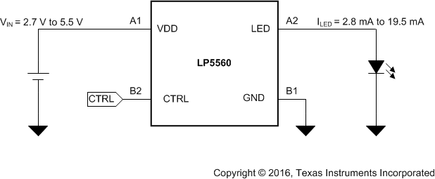 Figure 18. LP5560 Typical Application
8.2.1 Design Requirements
In this example LP5560 is used to drive a blue 0406-size indicator LED with a 5.3-mA output current. For this example, use the parameters listed in Table 7.
Table 7. Design Parameters
| DESIGN PARAMETER | EXAMPLE VALUE |
|---|---|
| LED Output Current | 5.3 mA |
| Maximum LED forward voltage at 5 mA | 3.1 V |
| VIN voltage | from 3.2 V to 5.5 V |
8.2.2 Detailed Design Procedure
8.2.2.1 Step-by-Step Design Procedure
To design in the LP5560 use the following simple design steps:
- Define the input voltage range of the system. For the LP5560 device the maximum input voltage must not exceed 5.5 V. The minimum input voltage is critical parameter for LED selection.
- Define the LED current. LED current affects the LED forward voltage and must be taken into account when selecting the LED for the application.
- Choose a LED which maximum forward voltage with desired LED current is less than minimum input voltage - 100 mV. This ensures that there is always enough headroom voltage available for the LED driver.
8.2.2.2 Running the Default Blinking Sequence
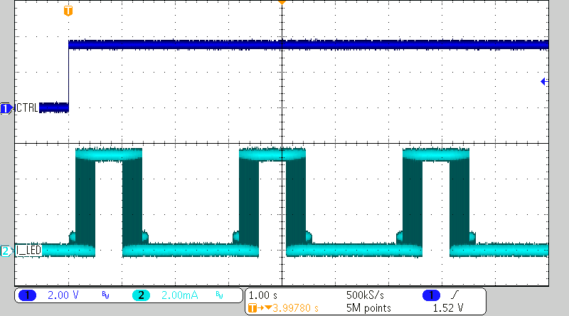
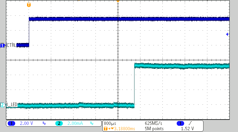
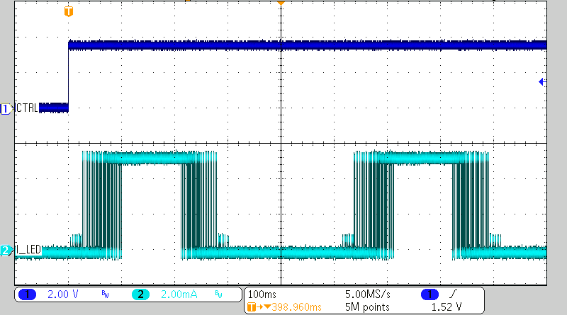
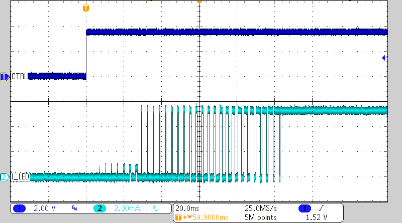
To run the default blinking sequence apply input voltage to VDD pin. Allow the VDD voltage settle before pulling the CTRL pin high. It is not recommended to connect the CTRL and VDD lines together. When CTRL line is pulled high the LP5560 starts to generate the default blinking sequence. Figure 19 shows the LP5560 generating default sequence. Rise and fall times are generated using a combined PWM and current control. Ramp has 32 PWM steps. For the first 8 steps LED current is decreased to 12.5%. For the remaining steps current is set to 100%. Each step is 3.3 ms long. This result’s the minimum ramp time of 3.3 ms × 32 = 105.6 ms. Figure 22 shows LED current with minimum rise time. When ramp time is increased each PWM step is done multiple times. In the default sequence rise and fall times are set to 528 ms.
8.2.2.3 Programming New Blinking Sequence to the Memory
Figure 22 shows an example of a training sequence which programs a new blinking sequence into the LP5560 memory. This example has a single pulse with 105.6 ms rise time, 105.6 ms on time, 105.6 ms fall time and 211.2 ms off time. LED current is set to 5.3 mA. Training sequence is started by giving a training start command (two rising edges within 500 µs). First pulse after a training start command is the calibration pulse which determines the speed of the training sequence. Note that there must always be at least 1500 µs from the first rising edge of the training start command before calibration pulse can be given. Second pulse after the calibration pulse is the LED current setting. Note that there are empty low times before and after current setting pulse. For the following pulses both CTRL high and CTRL low times are used to set the parameters. Next CTRL high time defines LED current rise time setting for pulse 1 (R1). CTRL low time after R1 defines the LED on time for pulse 1 (ON1). CTRL high time after ON1 sets the LED current fall time (F1). CTRL low time after F1 sets pulse 1 off time (OFF1). The training sequence is finished with a training stop command (three rising edges within 500 µs). Figure 23 show the LED current after programming the new pulse into the LP5560 memory.
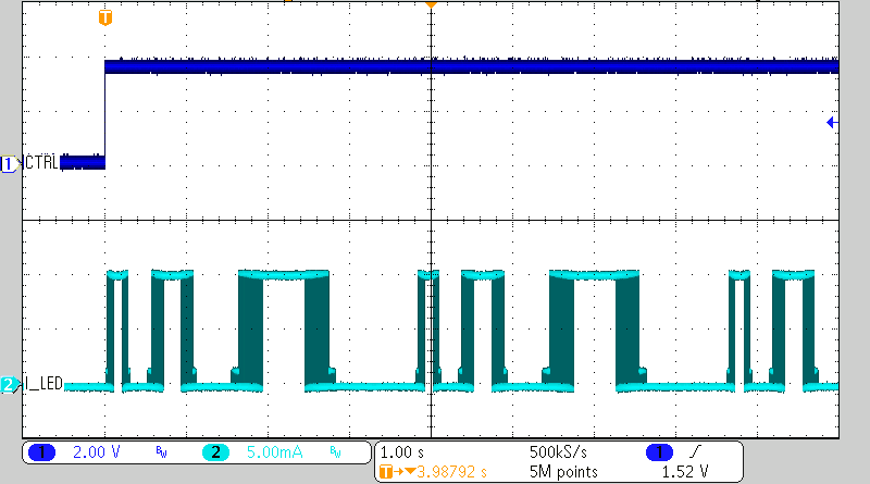
Figure 24 and Figure 25 show another example of a training sequence with three pulses and the resulting blinking sequence. In this example all three pulses have different rise, on, fall, and off times. LED current is set to 10.2 mA. Figure 26 show how this sequence is run only once using the run-once command. Even though the CTRL is held high for a long time the blinking sequence is only executed one time because a run-once command (four rising edges within 500 µs) is given at the beginning of the frame.
8.2.3 Application Curves
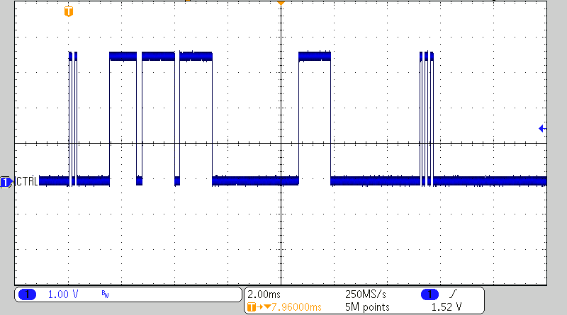
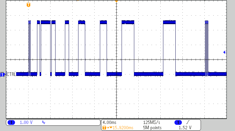
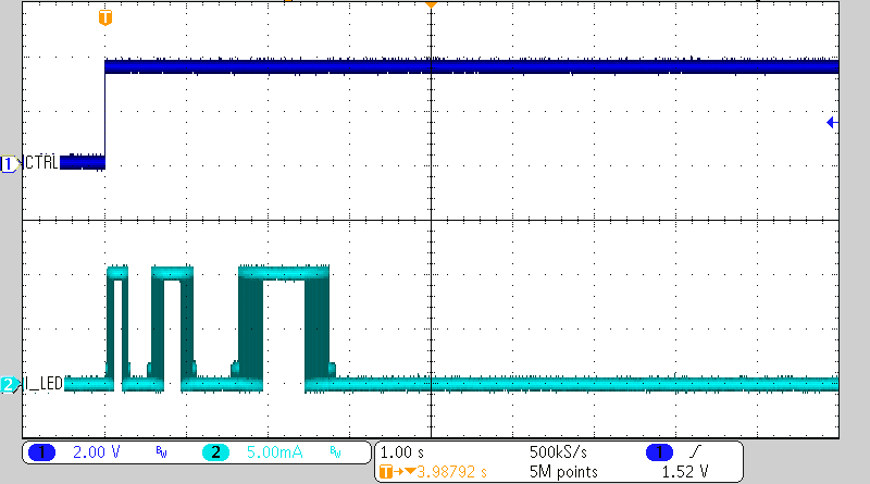
9 Power Supply Recommendations
The LP5560 is designed to operate from an input voltage supply range between 2.7 V and 5.5 V. This input supply must be well regulated. If the input voltage has high noise content TI recommends adding a dedicated ceramic bypass capacitor close to the VDD and GND pins. Depending on the selected LED it may be necessary to increase the minimum input voltage. The minimum input voltage must always be 100 mV higher than the LED maximum forward voltage.
10 Layout
10.1 Layout Guidelines
- Normally the LP5560 device does not require any external components except for the LED. However, in a noisy environment a small 0.1-µF bypass capacitor can be connected between VIN and GND pins.
- TI recommends routing the pins in a 45-degree angle to avoid component rotation during soldering process.
- Use traces with similar width for all pins. This makes the exposed copper area similar for all pins and improves the soldering reliability.
- Obtain the minimum clearance and trace width from the manufacturer of the PCB used for the board.
10.2 Layout Example
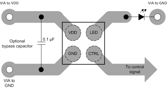 Figure 27. LP5560 Layout Example
11 器件和文档支持
11.1 文档支持
11.2 接收文档更新通知
如需接收文档更新通知,请访问 www.ti.com.cn 网站上的器件产品文件夹。点击右上角的提醒我 (Alert me) 注册后,即可每周定期收到已更改的产品信息。有关更改的详细信息,请查阅已修订文档中包含的修订历史记录。
11.3 社区资源
The following links connect to TI community resources. Linked contents are provided "AS IS" by the respective contributors. They do not constitute TI specifications and do not necessarily reflect TI's views; see TI's Terms of Use.
-
TI E2E™ Online Community TI's Engineer-to-Engineer (E2E) Community. Created to foster collaboration among engineers. At e2e.ti.com, you can ask questions, share knowledge, explore ideas and help solve problems with fellow engineers.
-
Design Support TI's Design Support Quickly find helpful E2E forums along with design support tools and contact information for technical support.
11.4 商标
E2E is a trademark of Texas Instruments.
All other trademarks are the property of their respective owners.
11.5 静电放电警告

ESD 可能会损坏该集成电路。德州仪器 (TI) 建议通过适当的预防措施处理所有集成电路。如果不遵守正确的处理措施和安装程序 , 可能会损坏集成电路。
ESD 的损坏小至导致微小的性能降级 , 大至整个器件故障。 精密的集成电路可能更容易受到损坏 , 这是因为非常细微的参数更改都可能会导致器件与其发布的规格不相符。
11.6 Glossary
SLYZ022 — TI Glossary.
This glossary lists and explains terms, acronyms, and definitions.
12 机械、封装和可订购信息
以下页中包括机械、封装和可订购信息。这些信息是针对指定器件可提供的最新数据。这些数据会在无通知且不对本文档进行修订的情况下发生改变。欲获得该数据表的浏览器版本,请查阅左侧的导航栏。
重要声明
德州仪器(TI) 及其下属子公司有权根据 JESD46 最新标准, 对所提供的产品和服务进行更正、修改、增强、改进或其它更改, 并有权根据 JESD48最新标准中止提供任何产品和服务。客户在下订单前应获取最新的相关信息, 并验证这些信息是否完整且是最新的。所有产品的销售都遵循在订单确认时所提供的TI 销售条款与条件。
TI 保证其所销售的组件的性能符合产品销售时 TI 半导体产品销售条件与条款的适用规范。仅在 TI 保证的范围内,且 TI 认为有必要时才会使用测试或其它质量控制技术。除非适用法律做出了硬性规定,否则没有必要对每种组件的所有参数进行测试。
TI 对应用帮助或客户产品设计不承担任何义务。客户应对其使用 TI 组件的产品和应用自行负责。为尽量减小与客户产品和应用相关的风险,客户应提供充分的设计与操作安全措施。
TI 不对任何 TI 专利权、版权、屏蔽作品权或其它与使用了 TI 组件或服务的组合设备、机器或流程相关的 TI 知识产权中授予 的直接或隐含权限作出任何保证或解释。TI所发布的与第三方产品或服务有关的信息,不能构成从 TI 获得使用这些产品或服 务的许可、授权、或认可。使用此类信息可能需要获得第三方的专利权或其它知识产权方面的许可,或是 TI 的专利权或其它知识产权方面的许可。
对于 TI 的产品手册或数据表中 TI 信息的重要部分,仅在没有对内容进行任何篡改且带有相关授权、条件、限制和声明的情况 下才允许进行复制。TI 对此类篡改过的文件不承担任何责任或义务。复制第三方的信息可能需要服从额外的限制条件。
在转售 TI 组件或服务时,如果对该组件或服务参数的陈述与 TI 标明的参数相比存在差异或虚假成分,则会失去相关 TI 组件或服务的所有明示或暗示授权,且这是不正当的、欺诈性商业行为。TI 对任何此类虚假陈述均不承担任何责任或义务。
客户认可并同意,尽管任何应用相关信息或支持仍可能由 TI 提供,但他们将独力负责满足与其产品及在其应用中使用 TI 产品相关的所有法律、法规和安全相关要求。客户声明并同意,他们具备制定与实施安全措施所需的全部专业技术和知识,可预见故障的危险后果、监测故障及其后果、降低有可能造成人身伤害的故障的发生机率并采取适当的补救措施。客户将全额赔偿因 在此类安全关键应用中使用任何 TI 组件而对 TI及其代理造成的任何损失。
在某些场合中,为了推进安全相关应用有可能对 TI 组件进行特别的促销。TI 的目标是利用此类组件帮助客户设计和创立其特有的可满足适用的功能安全性标准和要求的终端产品解决方案。尽管如此,此类组件仍然服从这些条款。
TI 组件未获得用于 FDA Class III(或类似的生命攸关医疗设备)的授权许可,除非各方授权官员已经达成了专门管控此类使 用的特别协议。
只有那些 TI 特别注明属于军用等级或“增强型塑料”的 TI 组件才是设计或专门用于军事/航空应用或环境的。购买者认可并同 意,对并非指定面向军事或航空航天用途的 TI组件进行军事或航空航天方面的应用,其风险由客户单独承担,并且由客户独 力负责满足与此类使用相关的所有法律和法规要求。
TI 已明确指定符合 ISO/TS16949 要求的产品,这些产品主要用于汽车。在任何情况下,因使用非指定产品而无法达到 ISO/TS16949要求,TI不承担任何责任。
产品
- 数字音频: www.ti.com.cn/audio
- 放大器和线性器件: www.ti.com.cn/amplifiers
- 数据转换器: www.ti.com.cn/dataconverters
- DLP® 产品: www.dlp.com
- DSP - 数字信号处理器: www.ti.com.cn/dsp
- 时钟和计时器: www.ti.com.cn/clockandtimers
- 接口: www.ti.com.cn/interface
- 逻辑: www.ti.com.cn/logic
- 电源管理: www.ti.com.cn/power
- 微控制器 (MCU): www.ti.com.cn/microcontrollers
- RFID 系统: www.ti.com.cn/rfidsys
- OMAP应用处理器: www.ti.com/omap
- 无线连通性: www.ti.com.cn/wirelessconnectivity
应用
- 通信与电信: www.ti.com.cn/telecom
- 计算机及周边: www.ti.com.cn/computer
- 消费电子: www.ti.com/consumer-apps
- 能源: www.ti.com/energy
- 工业应用: www.ti.com.cn/industrial
- 医疗电子: www.ti.com.cn/medical
- 安防应用: www.ti.com.cn/security
- 汽车电子: www.ti.com.cn/automotive
- 视频和影像: www.ti.com.cn/video
德州仪器在线技术支持社区: www.deyisupport.com
邮寄地址: 上海市浦东新区世纪大道1568 号,中建大厦32 楼邮政编码: 200122
Copyright© 2016, 德州仪器半导体技术(上海)有限公司