-
LDC1101 1.8V 高分辨率、高速电感数字转换器
- 1 特性
- 2 应用
- 3 说明
- 4 简化电路原理图
- 5 修订历史记录
- 6 Pin Configuration and Functions
- 7 Specifications
-
8 Detailed Description
- 8.1 Overview
- 8.2 Functional Block Diagram
- 8.3 Feature Description
- 8.4
Device Functional Modes
- 8.4.1 Measurement Modes
- 8.4.2 RP+L Measurement Mode
- 8.4.3 High Resolution L (LHR) Measurement Mode
- 8.4.4 Reference Count Setting
- 8.4.5 L-Only Measurement Operation
- 8.4.6 Minimum Sensor Frequency and Watchdog Setting
- 8.4.7 Low Power Modes
- 8.4.8 Status Reporting
- 8.4.9 Switch Functionality and INTB Reporting
- 8.5 Programming
- 8.6
Register Maps
- 8.6.1 Individual Register Listings
- 8.6.2 Register RP_SET (address = 0x01) [reset = 0x07]
- 8.6.3 Register TC1 (address = 0x02) [reset = 0x90]
- 8.6.4 Register TC2 (address = 0x03) [reset = 0xA0]
- 8.6.5 Register DIG_CONF (address = 0x04) [reset = 0x03]
- 8.6.6 Register ALT_CONFIG (address = 0x05) [reset = 0x00]
- 8.6.7 Register RP_THRESH_HI_LSB (address = 0x06) [reset = 0x00]
- 8.6.8 Register RP_THRESH_HI_MSB (address = 0x07) [reset = 0x00]
- 8.6.9 Register RP_THRESH_LO_LSB (address = 0x08) [reset = 0x00]
- 8.6.10 Register RP_THRESH_LO_MSB (address = 0x09) [reset = 0x00]
- 8.6.11 Register INTB_MODE (address = 0x0A) [reset = 0x00]
- 8.6.12 9.Register START_CONFIG (address = 0x0B) [reset = 0x01]
- 8.6.13 Register D_CONFIG (address = 0x0C) [reset = 0x00]
- 8.6.14 Register L_THRESH_HI_LSB (address = 0x16) [reset = 0x00]
- 8.6.15 Register L_THRESH_HI_MSB (address = 0x17) [reset = 0x00]
- 8.6.16 Register L_THRESH_LO_LSB (address = 0x18) [reset = 0x00]
- 8.6.17 Register L_THRESH_LO_MSB (address = 0x19) [reset = 0x00]
- 8.6.18 Register STATUS (address = 0x020 [reset = 0x00]
- 8.6.19 Register RP_DATA_LSB (address = 0x21) [reset = 0x00]
- 8.6.20 Register RP_DATA_MSB (address = 0x22) [reset = 0x00]
- 8.6.21 Register L_DATA_LSB (address = 0x23) [reset = 0x00]
- 8.6.22 Register L_DATA_MSB (address = 0x24) [reset = 0x00]
- 8.6.23 Register LHR_RCOUNT_LSB (address = 0x30) [reset = 0x00]
- 8.6.24 Register LHR_RCOUNT_MSB (address = 0x31) [reset = 0x00]
- 8.6.25 Register LHR_OFFSET_LSB (address = 0x32) [reset = 0x00]
- 8.6.26 Register LHR_OFFSET_MSB (address = 0x33) [reset = 0x00]
- 8.6.27 Register LHR_CONFIG (address = 0x34) [reset = 0x00]
- 8.6.28 Register LHR_DATA_LSB (address = 0x38) [reset = 0x00]
- 8.6.29 Register LHR_DATA_MID (address = 0x39) [reset = 0x00]
- 8.6.30 Register LHR_DATA_MSB (address = 0x3A) [reset = 0x00]
- 8.6.31 Register LHR_STATUS (address = 0x3B) [reset = 0x00]
- 8.6.32 Register RID (address = 0x3E) [reset = 0x02]
- 8.6.33 Register DEVICE_ID (address = 0x3F) [reset = 0xD4]
-
9 Application and Implementation
- 9.1
Application Information
- 9.1.1 Theory of Operation
- 9.1.2 RP+L Mode Calculations
- 9.1.3 LDC1101 RP Configuration
- 9.1.4 Setting Internal Time Constant 1
- 9.1.5 Setting Internal Time Constant 2
- 9.1.6 MIN_FREQ and Watchdog Configuration
- 9.1.7 RP+L Sample Rate Configuration with RESP_TIME
- 9.1.8 High Resolution Inductance Calculation (LHR mode)
- 9.1.9 LHR Sample Rate Configuration with RCOUNT
- 9.1.10 Setting RPMIN for LHR Measurements
- 9.1.11 Sensor Input Divider
- 9.1.12 Reference Clock Input
- 9.1.13 INTB Reporting on SDO
- 9.1.14 DRDY (Data Ready) Reporting on SDO
- 9.1.15 Comparator Functionality
- 9.2 Typical Application
- 9.1
Application Information
- 10Power Supply Recommendations
- 11Layout
- 12器件和文档支持
- 13机械、封装和可订购信息
- 重要声明
LDC1101 1.8V 高分辨率、高速电感数字转换器
1 特性
2 应用
- 高速轮齿计数
- 高速事件计数
- 电机转速感测
- 家用电器、汽车和消费类应用中的旋钮和拨盘
- 家用电器、汽车和消费类应用中的人机界面 (HMI)
- 按钮和键盘
- 电机控制
- 金属探测
3 说明
LDC1101 是一款 1.8V 至 3.3V、高分辨率电感数字转换器,可对位置、旋转或运动进行短距离、高速、无触点感测,即使存在污垢或灰尘也能够实现可靠、精确的测量,非常适合户外或严苛环境。
LDC1101 特有双感应测量内核,可在执行 > 150ksps 的 16 位 RP 和 L 测量的同时,进行分辨率高达 24 位的高分辨率 L 测量,采样速率可高达 180ksps 以上。 LDC1101 包含阈值比较功能,该功能可在器件运行时动态更新。
电感感测技术可实现对线性/角位置、位移、运动、压缩、振动、金属成分以及市面上包括汽车、消费类、计算机、工业、医疗和通信应用在内的很多其他应用的高精度测量。 电感感测技术能够以低于其他竞争对手解决方案的成本提供更为出色的性能和可靠性。
LDC1101 在小型 3mm × 3mm 10 引脚 VSON 封装内即可提供这些电感感测技术优势。 微控制器可使用 4 引脚 SPI™轻松配置 LDC1101。
器件信息(1)
| 器件型号 | 封装 | 封装尺寸(标称值) |
|---|---|---|
| LDC1101 | VSON (10) | 3.00mm × 3.00mm |
- 如需了解所有可用封装,请见数据表末尾的可订购产品附录。
4 简化电路原理图
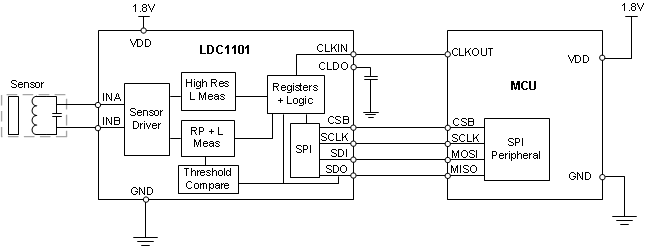
6 Pin Configuration and Functions
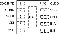
Pin Functions
| PIN | TYPE(1) | DESCRIPTION | |
|---|---|---|---|
| NAME | NO. | ||
| CLDO | 10 | P | Internal LDO bypassing pin. A 15 nF capacitor must be connected from this pin to GND. |
| CLKIN | 2 | I | External time-base Clock Input |
| CSB | 5 | I | SPI CSB. Multiple devices can be connected on the same SPI bus and CSB can be used to uniquely select desired device |
| DAP | – | – | Connect to Ground for improved thermal performance(2) |
| GND | 8 | G | Ground |
| INA | 7 | A | External LC tank – connected to external LC tank |
| INB | 6 | A | External LC tank – connected to external LC tank |
| SCLK | 3 | I | SPI Clock Input |
| SDI | 4 | I | SPI Data Input – connect to MOSI of SPI master |
| SDO/INTB | 1 | O | SPI Data Output/INTB – Connect to MISO of SPI Master. When CSB is high, this pin is High-Z. Alternatively, this pin can be configured to function as INTB |
| VDD | 9 | P | Power Supply |
7 Specifications
7.1 Absolute Maximum Ratings
over operating free-air temperature range (unless otherwise noted)(1)| MIN | MAX | UNIT | ||
|---|---|---|---|---|
| VDD | Supply voltage range | 3.6 | V | |
| Vi | Voltage on INA, INB | –0.3 | 2.3 | V |
| Voltage on CLDO | –0.3 | 1.9 | V | |
| Voltage on any other pin(2) | –0.3 | VDD+0.3 | V | |
| TJ | Junction temperature | –55 | 125 | °C |
| Tstg | Storage temperature | –65 | 125 | °C |
7.2 ESD Ratings
| VALUE | UNIT | |||
|---|---|---|---|---|
| V(ESD) | Electrostatic discharge | Human-body model (HBM), per ANSI/ESDA/JEDEC JS-001(1) | ±2000 | V |
| Charged-device model (CDM), per JEDEC specification JESD22-C101(2) | ±1000 | |||
7.3 Recommended Operating Conditions
over operating free-air temperature range (unless otherwise noted)| MIN | NOM | MAX | UNIT | ||
|---|---|---|---|---|---|
| VDD | Supply voltage | 1.71 | 3.46 | V | |
| TJ | Junction temperature | –40 | 125 | °C | |
7.4 Thermal Information
| THERMAL METRIC(1) | LDC1101 | UNIT | |
|---|---|---|---|
| DRC (VSON) | |||
| 10 PINS | |||
| RθJA | Junction-to-ambient thermal resistance | 44.2 | °C/W |
| RθJC(top) | Junction-to-case (top) thermal resistance | 50.1 | °C/W |
| RθJB | Junction-to-board thermal resistance | 19.6 | °C/W |
| ψJT | Junction-to-top characterization parameter | 0.7 | °C/W |
| ψJB | Junction-to-board characterization parameter | 19.8 | °C/W |
| RθJC(bot) | Junction-to-case (bottom) thermal resistance | 4.4 | °C/W |
7.5 Electrical Characteristics
Over recommended operating conditions unless otherwise noted. VDD = 1.8 V, TA = 25°C.| PARAMETER | TEST CONDITION(1) | MIN(2) | TYP(3) | MAX(2) | UNIT | |
|---|---|---|---|---|---|---|
| POWER | ||||||
| VDD | Supply voltage | 1.71 | 3.46 | V | ||
| IDD | Supply current | START_CONFIG= 0x00, no sensor connected | 1.9 | 2.7 | mA | |
| IDDS | Supply current including sensor current | ƒCLKIN = 16 MHz, ƒSENSOR = 2 MHz, START_CONFIG = 0x00 |
3.2 | mA | ||
| IDDSL | Sleep mode supply current | START_CONFIG =0x01 | 135 | 180 | µA | |
| ISD | Shutdown mode supply current | 1.4 | 6.7 | µA | ||
| SENSOR | ||||||
| RP Measurement part-to-part variation | RESP_TIME= 6144, D_CONFIG=0x00, ALT_CONFIG=0x00, START_CONFIG = 0x00, ƒSENSOR = 2 MHz | 1% | ||||
| ISENSORMAX | Sensor maximum current drive | RP_MIN = b111, START_CONFIG=0x00, D_CONFIG=0x00, ALT_CONFIG=0x00 | 0.598 | 0.6 | 0.602 | mA |
| ISENSORMIN | Sensor minimum current drive | RP_MAX = b000, RPMAX_DIS=b0, START_CONFIG=0x00, D_CONFIG=0x00, ALT_CONFIG=0x00 | 4.7 | µA | ||
| ƒSENSOR | Sensor resonant frequency | Device settings and Sensor compliant as detailed in LDC1101 RP Configuration | 0.5 | 10 | MHz | |
| RPRES | RP Measurement resolution | 16 | bits | |||
| LRES | Inductance sensing resolution – RP+L Mode | 16 | bits | |||
| Inductance sensing resolution – LHR Mode | 24 | bits | ||||
| AOSC | Sensor oscillation amplitude | INA – INB, START_CONFIG=0x00, D_CONFIG=0x00, ALT_CONFIG=0x00 | 1.2 | VPP | ||
| DETECTION | ||||||
| tS_MIN | Minimum response time (RP+L mode) | RP+L Mode, RESP_TIME=b010 | 192 ÷ƒSENSOR |
s | ||
| tS_MAX | Maximum response time (RP+L mode) | RP+L Mode, RESP_TIME=b111 | 6144 ÷ƒSENSOR |
s | ||
| Ts_MAX | High Res L maximum measurement interval | LHR_REF_COUNT=0xFFFF, START_CONFIG=0x00 | (220+39) ÷ƒCLKIN |
s | ||
| SRMAXRP | RP+L Mode maximum sample rate | ƒCLKIN=16 MHz, ƒSENSOR = 10 MHz, RESP_TIME=b010 | 156.25 | kSPS | ||
| SRMAXL | High Res L Mode Maximum Sample Rate | High Resolution L Mode, LHR_REF_COUNT=0x0002, ƒCLKIN=16 MHz | 183.8 | kSPS | ||
| FREQUENCY REFERENCE | ||||||
| fCLKIN | Reference input frequency | 1 | 16 | MHz | ||
| DCfin | Reference duty cycle | 40% | 60% | |||
| VIH | Input high voltage (Logic “1”) | 0.8×VDD | V | |||
| VIL | Input low voltage (Logic “0”) | 0.2×VDD | V | |||
7.6 Digital Interface
| PARAMETER | MIN | TYP | MAX | UNIT | |
|---|---|---|---|---|---|
| VOLTAGE LEVELS | 0.8×VDD | V | |||
| VIH | Input high voltage (Logic “1”) | 0.2×VDD | V | ||
| VIL | Input low voltage (Logic “0”) | VDD–0.3 | V | ||
| VOH | Output high voltage (Logic “1”, ISOURCE = 400 µA) | 0.3 | V | ||
| VOL | Output low voltage (Logic “0”, ISINK = 400 µA) | –500 | 500 | nA | |
| IOHL | Digital IO leakage current | ||||
7.7 Timing Requirements
| MIN | TYP | MAX | UNIT | ||
|---|---|---|---|---|---|
| tSTART | Start-up time from shutdown to sleep | 0.8 | ms | ||
| tWAKE | Wake-up time (from completion of SPI to conversion start; does not include sensor settling time) | 0.04 | ms | ||
| INTERFACE TIMING REQUIREMENTS(1) | |||||
| ƒSCLK | Serial clock frequency | 8 | MHz | ||
| twH | SCLK pulse-width high | 0.4 / ƒSCLK | s | ||
| twL | SCLK pulse-width low | 0.4 / ƒSCLK | s | ||
| tsu | SDI setup time | 10 | ns | ||
| th | SDI hold time | 10 | ns | ||
| tODZ | SDO driven-to-tristate time | 25 | ns | ||
| tOZD | SDO tristate-to-driven time | 25 | ns | ||
| tOD | SDO output delay time | 20 | ns | ||
| tsu(CS) | CSB setup time | 20 | ns | ||
| th(CS) | CSB hold time | 20 | ns | ||
| tIAG | CSB inter-access interval | 100 | ns | ||
| tw(DRDY) | Data ready pulse width | 1/ƒSENSOR | ns | ||
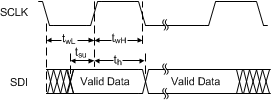 Figure 1. Write Timing Diagram
 Figure 2. Read Timing Diagram
7.8 Typical Characteristics
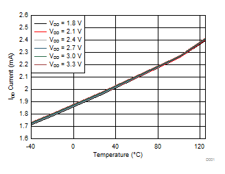
| Not including sensor current, default register settings. |
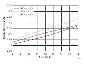
| Including sensor current. 13mm diameter sensor 0.1mm spacing/0.1mm trace width/ 4 layer 28 turns, fSENSOR = 2 MHz, RP_SET = 0x07, TX1=0x50, TC2=0x80, RCOUNT=0xFFFF, RESP_TIME =6144 |
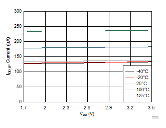
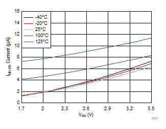

| RP_SET.RPMAX = b000 |
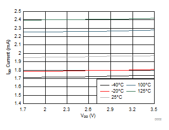
| Not including sensor current, default register settings. |
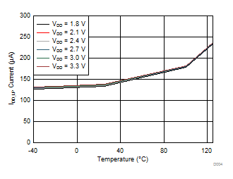
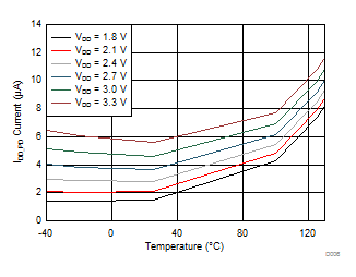

| RP_SET.RPMIN = b111 |
8 Detailed Description
8.1 Overview
The LDC1101 is an inductance-to-digital converter which can simultaneously measure the impedance and resonant frequency of an LC resonator. The high resolution measurement capability enables this device to be used to directly measure changes in physical systems, allowing the resonator to sense the proximity and movement of conductive materials.
The LDC1101 measures the impedance and resonant frequency by regulating the oscillation amplitude in a closed-loop configuration at a constant level, while monitoring the energy dissipated by the resonator. By monitoring the amount of power injected into the resonator, the LDC1101 can determine the equivalent parallel resistance of the resonator, RP, which it returns as a digital value.
In addition, the LDC1101 device also measures the oscillation frequency of the LC circuit by comparing the sensor frequency to a provided reference frequency. The sensor frequency can then be used to determine the inductance of the LC circuit.
The threshold comparator block can compare the RP+L conversion results versus a programmable threshold. With the threshold registers programmed and comparator enabled, the LDC1101 can provide a switch output, reported as a high/low level on the INTB/SDO pin.
The LDC1101 device supports a wide range of LC combinations with oscillation frequencies ranging from 500 kHz to 10 MHz and RP ranging from 1.25 kΩ to 90 kΩ. The device is configured and conversion results retrieved through a simple 4-wire SPI. The power supply for the device can range from 1.8 V – 5% to 3.3 V + 5%. The only external components necessary for operation are a 15 nF capacitor for internal LDO bypassing and supply bypassing for VDD.
8.2 Functional Block Diagram

8.3 Feature Description
8.3.1 Sensor Driver
The LDC1101 can drive a sensor with a resonant frequency of 500 kHz to 10 MHz with an RP in the range of 1.25 kΩ to 90 kΩ. The nominal sensor amplitude is 1.2 V. The sensor Q should be at least 10 for RP measurements. The inductive sensor must be connected across the INA and INB pins. The resonant frequency of the sensor is set by:

where
- L is the sensor inductance in Henrys, and
- C is the sensor parallel capacitance in Farads.
8.4 Device Functional Modes
8.4.1 Measurement Modes
The LDC1101 features two independent measurement subsystems to measure the impedance and resonant frequency of an attached sensor. The RP+L subsystem can simultaneously measure the impedance and resonant frequency of an LC resonator, with up to 16 bits of resolution for each parameter. Refer to RP+L Measurement Mode for more information on the RP+L measurement functionality.
The High Resolution L (LHR) subsystem measures the sensor resonant frequency with up to 24 bits of resolution. The effective resolution is a function of the sample rate and the reference frequency supplied on the CLKIN pin. Refer to High Resolution L (LHR) Measurement Mode for more information on the LHR measurement functionality.
Both measurement subsystems can convert simultaneously but at different sample intervals – the completion of an RP+L conversion will be asynchronous to the completion of a LHR conversion.
Table 1. Comparison of Measurement Modes
| RP+L Mode | LHR Mode | |
|---|---|---|
| RP Measurement Resolution | 16 bits | N/A |
| L Measurement Resolution | 16 bits | 24 bits |
| Sample Rate configuration | Varies with ƒSENSOR, set by RESP_TIME | Fixed and set by RCOUNT field and ƒCLKIN |
| Sample rate at highest resolution (SPS) | 244 | 15.3 |
| Maximum Sample Rate (kSPS) | 156.25 | 183.9 |
| L Resolution at Maximum Sample rate | 6.7 bits | 6.5 bits |
| Switch Output on SDO/INTB | Available for RP or L output code | N/A |
8.4.2 RP+L Measurement Mode
In RP+L mode, the LDC1101 will simultaneously measure the impedance and resonant frequency of the attached sensor. The device accomplishes this task by regulating the oscillation amplitude in a closed-loop configuration to a constant level, while monitoring the energy dissipated by the resonator. By monitoring the amount of power injected into the resonator, the LDC1101 device can determine the value of RP. The device returns this value as a digital value which is proportional to RP. In addition, the LDC1101 device can also measure the oscillation frequency of the LC circuit, by counting the number of cycles of a reference frequency. The measured sensor frequency can be used to determine the inductance of the LC circuit.
8.4.2.1 RPMIN and RPMAX
The variation of RP in a given system is typically much smaller than maximum range of 1.25 kΩ to >90 kΩ supported by the LDC1101. To achieve better resolution for systems with smaller RP ranges, the LDC1101 device offers a programmable RP range.
The LDC1101 uses adjustable current drives to scale the RP measurement range; by setting a tighter current range a higher accuracy RP measurement can be performed. This functionality can be considered as a variable gain amplifier (VGA) front end to an ADC. The current ranges are configured in the RPMIN and RPMAX fields of register RP_SET (address 0x01). Refer to LDC1101 RP Configuration for instructions to optimize these settings.
8.4.2.2 Programmable Internal Time Constants
The LDC1101 utilizes internal programmable registers to configure time constants necessary for sensor oscillation. These internal time constants must be configured for RP measurements. Refer to Setting Internal Time Constant 1 and Setting Internal Time Constant 2 for instructions on how to configure them for a given system.
8.4.2.3 RP+L Mode Measurement Sample Rate
The LDC1101 provides an adjustable sample rate for the RP+L conversion, where longer conversion times have higher resolution. Refer to RP+L Sample Rate Configuration with RESP_TIME for more details.
8.4.3 High Resolution L (LHR) Measurement Mode
The High Resolution L measurement (LHR) subsystem provides a high-resolution inductance (L) measurement of up to 24 bits. This L measurement can be configured to provide a higher resolution measurement than the measurement returned from the RP+L subsystem. The LHR subsystem also provides a constant conversion time interval, whereas the RP+L conversion interval is a function of the sensor frequency. The LHR measurement runs asynchronously with respect to the RP+L measurement.
8.4.4 Reference Count Setting
The LHR sample rate is set by the Reference Count (LHR_RCOUNT) setting (registers 0x30 and 0x31). The LHR conversion resolution is proportional to the programmed RCOUNT value. With the maximum supported 16 MHz CLKIN input, the LDC1101 conversion interval can be set from 8.6 µs to 87.38 ms in 1 µs increments. Note that longer conversion intervals produce more accurate LHR measurements. Refer to LHR Sample Rate Configuration with RCOUNT for more details.
8.4.5 L-Only Measurement Operation
The LDC1101 can disable the RP measurement to perform a more stable L measurement. To enable this mode, set:
- ALT_CONFIG.LOPTIMAL(register 0x05-bit0) = 1
- D_CONFIG.DOK_REPORT (register 0x0C-bit0) = 1
When this mode is used, RP measurement results are not valid.
8.4.6 Minimum Sensor Frequency and Watchdog Setting
The LDC1101 can report an error condition if the sensor oscillation stops. Refer to MIN_FREQ and Watchdog Configuration for information on the configuration of the watchdog.
8.4.7 Low Power Modes
When continuous LDC conversions are not required, the LDC1101 supports two reduced power modes. In Sleep mode, the LDC1101 retains register settings and can quickly enter active mode for conversions. In Shutdown mode, power consumption is significantly lower, although the device configuration is not retained. While in either low power mode, the LDC1101 will not perform conversions.
8.4.7.1 Shutdown Mode
Shutdown mode is the lowest power state for the LDC1101. Note that entering SD mode will reset all registers to their default state, and so the device must have its registers rewritten. To enter Shutdown, perform the following sequence:
- Set ALT_CONFIG.SHUTDOWN_EN = 1 (register 0x05-bit[1]).
- Stop toggling the CLKIN pin input and drive the CLKIN pin Low.
- Set START_CONFIG.FUNC_MODE = b10 (register 0x0B:bits[1:0]). This register can be written while the LDC1101 is in active mode; on completion of the register write the LDC1101 will enter shutdown.
To exit Shutdown mode, resume toggling the clock input on the CLKIN pin; the LDC1101 will transition to Sleep mode with the default register values.
While in Shutdown mode, no conversions are performed. In addition, entering Shutdown mode will clear the status registers; if an error condition is present it will not be reported when the device exits Shutdown mode.
8.4.7.2 Sleep Mode
Sleep mode is entered by setting START_CONFIG.FUNC_MODE =b01 (register 0x0B:bits[1:0]). While in this mode, the register contents are maintained. To exit Sleep mode and start active conversions, set START_CONFIG.FUNC_MODE = b00. While in Sleep mode the SPI interface is functional so that register reads and writes can be performed.
On power-up or exiting Shutdown mode, the LDC1101 will be in Sleep mode.
Configuring the LDC1101 must be done while the device is in Sleep mode. If a setting on the LDC1101 needs to be changed, return the device to Sleep mode, change the appropriate register, and then return the LDC1101 to conversion mode. The registers related to INTB reporting can be changed while the LDC1101 is in active mode. Refer to INTB Reporting on SDO for more details.
8.4.8 Status Reporting
The LDC1101 provides 2 status registers, STATUS and LHR_STATUS, to report on the device and sensor condition.
Table 2. STATUS Fields
| NAME | FIELD | FUNCTION |
|---|---|---|
| NO_SENSOR_OSC | 7 | When the resonance impedance of the sensor, RP, drops below the programed Rp_MIN, the sensor oscillation may stop. This condition is reported by STATUS:NO_SENSOR_OSC (register 0x20-bit7). This condition could occur when a target comes too close to the sensor or if RP_SET:RP_MIN (register 0x01-bits[2:0]) is set too high. |
| DRDYB | 6 | RP+L Data Ready - reports completion of RP+L conversion results |
| RP_HIN | 5 | RP+L threshold – refer to Comparator Functionalityfor details |
| RP_HI_LON | 4 | |
| L_HIN | 3 | |
| L_HI_LON | 2 | |
| POR_READ | 0 | Device in Power-On Reset – device should only be configured when POR_READ = 0. |
The LHR_STATUS register (register 0x3B) reports on LHR functionality.
8.4.9 Switch Functionality and INTB Reporting
The SDO pin can generate INTB, a signal which corresponds to device status. INTB can report conversion completion or provide a comparator output, in which the LDC conversion results are internally compared to programmable thresholds. Refer to INTB Reporting on SDO for details.
8.5 Programming
8.5.1 SPI Programming
The LDC1101 uses SPI to configure the internal registers. It is necessary to configure the LDC1101 while in Sleep mode. If a setting on the LDC1101 needs to be changed, return the device to Sleep mode, change the appropriate register, and then return the LDC1101 to conversion mode. CSB must go low before accessing first address. If the number of SCLK pulses is less than 16, a register write command will not change the contents of the addressed register.
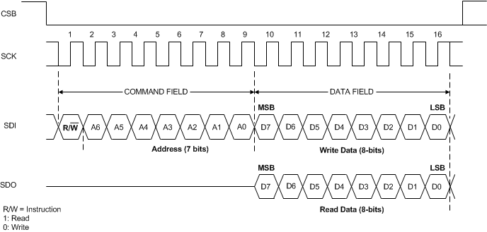 Figure 12. SPI Transaction Format
The LDC1101 supports an extended SPI transaction, in which CSB is held low and sequential register addresses can be written or read. After the first register transaction, each additional 8 SCLK pulses will address the next register, reading or writing based on the initial R/W flag in the initial command. A register write command will take effect on the 8th clock pulse. Two or more registers can be programmed using this method. The register address must not increment above 0x3F.
 Figure 13. Extended SPI Transaction
8.6 Register Maps
Table 3. Register List
| ADDRESS | NAME | DEFAULT VALUE | DESCRIPTION |
|---|---|---|---|
| 0x01 | RP_SET | 0x07 | Configure RP Measurement Dynamic Range |
| 0x02 | TC1 | 0x90 | Configure Internal Time Constant 1 |
| 0x03 | TC2 | 0xA0 | Configure Internal Time Constant 2 |
| 0x04 | DIG_CONFIG | 0x03 | Configure RP+L conversion interval |
| 0x05 | ALT_CONFIG | 0x00 | Configure additional device settings |
| 0x06 | RP_THRESH_H_LSB | 0x00 | RP_THRESHOLD High Setting – bits 7:0. This register can be modified while the LDC1101 is in active mode. |
| 0x07 | RP_THRESH_H_MSB | 0x00 | RP_THRESHOLD High Setting – bits 15:8. This register can be modified while the LDC1101 is in active mode. |
| 0x08 | RP_THRESH_L_LSB | 0x00 | RP_THRESHOLD Low Setting – bits 7:0. This register can be modified while the LDC1101 is in active mode. |
| 0x09 | RP_THRESH_L_MSB | 0x00 | RP_THRESHOLD Low Setting – bits 15:8. This register can be modified while the LDC1101 is in active mode. |
| 0x0A | INTB_MODE | 0x00 | Configure INTB reporting on SDO pin. This register can be modified while the LDC1101 is in active mode. |
| 0x0B | START_CONFIG | 0x01 | Configure Power State |
| 0x0C | D_CONF | 0x00 | Sensor Amplitude Control Requirement |
| 0x16 | L_THRESH_HI_LSB | 0x00 | L_THRESHOLD High Setting – bits 7:0. This register can be modified while the LDC1101 is in active mode. |
| 0x17 | L_THRESH_HI_MSB | 0x00 | L_THRESHOLD High Setting – bits 15:8. This register can be modified while the LDC1101 is in active mode. |
| 0x18 | L_THRESH_LO_LSB | 0x00 | L_THRESHOLD Low Setting – bits 7:0. This register can be modified while the LDC1101 is in active mode. |
| 0x19 | L_THRESH_LO_MSB | 0x00 | L_THRESHOLD Low Setting – bits 15:8. This register can be modified while the LDC1101 is in active mode. |
| 0x20 | STATUS | 0x00 | Report RP+L measurement status |
| 0x21 | RP_DATA_LSB | 0x00 | RP Conversion Result Data Output - bits 7:0 |
| 0x22 | RP_DATA_MSB | 0x00 | RP Conversion Result Data Output - bits 15:8 |
| 0x23 | L_DATA_LSB | 0x00 | L Conversion Result Data Output - bits 7:0 |
| 0x24 | L_DATA_MSB | 0x00 | L Conversion Result Data Output - bits 15:8 |
| 0x30 | LHR_RCOUNT_LSB | 0x00 | High Resolution L Reference Count – bits 7:0 |
| 0x31 | LHR_RCOUNT_MSB | 0x00 | High Resolution L Reference Count – bits 15:8 |
| 0x32 | LHR_OFFSET_LSB | 0x00 | High Resolution L Offset – bits 7:0 |
| 0x33 | LHR_OFFSET_MSB | 0x00 | High Resolution L Offset – bits 15:8 |
| 0x34 | LHR_CONFIG | 0x00 | High Resolution L Configuration |
| 0x38 | LHR_DATA_LSB | 0x00 | High Resolution L Conversion Result Data output - bits 7:0 |
| 0x39 | LHR_DATA_MID | 0x00 | High Resolution L Conversion Result Data output - bits 15:8 |
| 0x3A | LHR_DATA_MSB | 0x00 | High Resolution L Conversion Result Data output - bits 23:16 |
| 0x3B | LHR_STATUS | 0x00 | High Resolution L Measurement Status |
| 0x3E | RID | 0x02 | Device RID value |
| 0x3F | CHIP_ID | 0xD4 | Device ID value |
8.6.1 Individual Register Listings
Fields indicated with Reserved must be written only with indicated values. Improper device operation may occur otherwise. The R/W column indicates the Read-Write status of the corresponding field. A ‘R/W’ entry indicates read and write capability, a ‘R’ indicates read-only, and a ‘W’ indicates write-only.
8.6.2 Register RP_SET (address = 0x01) [reset = 0x07]
| 7 | 6 | 5 | 4 | 3 | 2 | 1 | 0 |
| RPMAX_DIS | RP_MAX | RESERVED | RP_MIN | ||||
| R/W | R/W | R/W | R/W | ||||
| LEGEND: R/W = Read/Write; R = Read only; -n = value after reset |
Table 4. Register RP_SET Field Descriptions
| Bit | Field | Type | Reset | Description |
|---|---|---|---|---|
| 7 | RPMAX_DIS | R/W | RP_MAX Disable
This setting improves the RP measurement accuracy for very high Q coils by driving 0A as the RPMAX current drive. b0: Programmed RP_MAX is driven (default value)
|
|
| 6:4 | RP_MAX | R/W | RP_MAX Setting
Set the maximum input dynamic range for the sensor RP measurement. The programmed RP_MIN setting must not exceed the programmed RP_MAX setting. b000: RPMAX = 96 kΩ (default value)b001: RPMAX = 48 kΩ b010: RPMAX = 24 kΩ b011: RPMAX = 12 kΩ b100: RPMAX = 6 kΩ b101: RPMAX = 3 kΩ b110: RPMAX = 1.5 kΩ b111: RPMAX = 0.75 kΩ |
|
| 3 | RESERVED | R/W | Reserved. Set to 0 | |
| 2:0 | RP_MIN | R/W | RP_MIN Setting
Set the minimum input dynamic range for the sensor RP measurement. The programmed RP_MIN setting must not exceed the programmed RP_MAX setting. b000: RPMIN = 96 kΩb001: RPMIN = 48 kΩ b010: RPMIN = 24 kΩ b011: RPMIN = 12 kΩ b100: RPMIN = 6 kΩ b101: RPMIN = 3 kΩ b110: RPMIN = 1.5 kΩ b111: RPMIN = 0.75 kΩ (default value) |
8.6.3 Register TC1 (address = 0x02) [reset = 0x90]
| 7 | 6 | 5 | 4 | 3 | 2 | 1 | 0 |
| C1 | RESERVED | R1 | |||||
| R/W | R/W | R/W | |||||
| LEGEND: R/W = Read/Write; R = Read only; -n = value after reset |
Table 5. Register TC1 Field Descriptions
| Bit | Field | Type | Reset | Description |
|---|---|---|---|---|
| 7:6 | C1 | R/W | Internal Time Constant 1 Capacitance
This sets the capacitive component used to configure internal time constant 1. Refer to Setting Internal Time Constant 1 for more details. b00: C1 = 0.75 pFb01: C1 = 1.5 pF b10: C1 = 3.0 pF (default value) b11: C1 = 6.0 pF |
|
| 5 | RESERVED | R/W | Reserved. Set to 0 | |
| 4:0 | R1 | R/W | Internal Time Constant 1 Resistance
This sets the resistive component used to configure internal time constant 1. Refer to Setting Internal Time Constant 1 for configuration details. R1(Ω) = -12.77 kΩ × R1 + 417 kΩ Valid Values: [b0’0000:b1’1111] |
8.6.4 Register TC2 (address = 0x03) [reset = 0xA0]
| 7 | 6 | 5 | 4 | 3 | 2 | 1 | 0 |
| C2 | R2 | ||||||
| R/W | R/W | ||||||
| LEGEND: R/W = Read/Write; R = Read only; -n = value after reset |
Table 6. Register TC2 Field Descriptions
| Bit | Field | Type | Reset | Description |
|---|---|---|---|---|
| 7:6 | C2 | R/W | Internal Time Constant 2 Capacitance
This sets the capacitive component used to configure internal time constant 2. Refer to Setting Internal Time Constant 2 for configuration details. b00: C2 = 3 pFb01: C2 = 6 pF b10: C2 = 12 pF (default value) b11: C2 = 24 pF |
|
| 5:0 | R2 | R/W | Internal Time Constant 2 Resistance
This sets the resistive component used to configure internal time constant 2. Refer to Setting Internal Time Constant 2for details. R2(Ω) = -12.77 kΩ × R2 + 835 kΩValid Values: [b00’0000:b11’1111] b00’0000: R2 = 835kΩ b10’0000: R2 = 426.4 kΩ (default value) b11’1111: R2 = 30.5 kΩ |
8.6.5 Register DIG_CONF (address = 0x04) [reset = 0x03]
| 7 | 6 | 5 | 4 | 3 | 2 | 1 | 0 |
| MIN_FREQ | RESERVED | RESP_TIME | |||||
| R/W | R/W | ||||||
| LEGEND: R/W = Read/Write; R = Read only; -n = value after reset |
Table 7. Register DIG_CONF Field Descriptions
| Bit | Field | Type | Reset | Description |
|---|---|---|---|---|
| 7:4 | MIN_FREQ | R/W | Sensor Minimum Frequency
Configure this register based on the lowest possible sensor frequency. This is typically when the target is providing minimum interaction with the sensor, although with some steel and ferrite targets, the minimum sensor frequency occurs with maximum target interaction. This setting should include any additional effects which reduce the sensor frequency, including temperature shifts and sensor capacitor variation. MIN_FREQ = 16 – (8 MHz ÷ ƒSENSORMIN) b0000: ƒSENSORMIN = 500 kHz (default value)
|
|
| 3 | RESERVED | R/W | Reserved. Set to 0 | |
| 2:0 | RESP_TIME | R/W | Measurement Response Time Setting
Sets the Response Time, which is the number of sensor periods used per conversion. This setting applies to the RP and Standard Resolution L measurement, but not the High Resolution L measurement. This corresponds to the actual conversion time by: 
b000: Reserved (do not use) |
8.6.6 Register ALT_CONFIG (address = 0x05) [reset = 0x00]
| 7 | 6 | 5 | 4 | 3 | 2 | 1 | 0 |
| RESERVED | SHUTDOWN_EN | LOPTIMAL | |||||
| R/W | R/W | R/W | |||||
| LEGEND: R/W = Read/Write; R = Read only; -n = value after reset |
Table 8. Register ALT_CONFIG Field Descriptions
| Bit | Field | Type | Reset | Description |
|---|---|---|---|---|
| 7:2 | RESERVED | R/W | Reserved. Set to b00'0000. | |
| 1 | SHUTDOWN_EN | R/W | Shutdown Enable
Enables shutdown mode of operation. If SHUTDOWN_EN is not set to 1, then SHUTDOWN (Address 0x0B:[1]) will not have any effect. b0: Shutdown not enabled. (default value) b1: Shutdown functionality enabled. |
|
| 0 | LOPTIMAL | R/W | Optimize for L Measurements
Optimize sensor drive signal for L measurements (for both High-Res L and L measurement). When LOPTIMAL is enabled, RP measurements will not be completed. It is also necessary to set DOK_REPORT=1 when this mode is enabled. b0: L optimal disabled; both RP+L/LHR measurements (default value)b1: Only perform LHR and/or L-only measurements. RP measurements are invalid. |
8.6.7 Register RP_THRESH_HI_LSB (address = 0x06) [reset = 0x00]
This register can be modified while the LDC1101 is in active mode.
| 7 | 6 | 5 | 4 | 3 | 2 | 1 | 0 |
| RP_THRESH_HI_LSB | |||||||
| R/W | |||||||
| LEGEND: R/W = Read/Write; R = Read only; -n = value after reset |
Table 9. Register RP_THRESH_HI_LSB Field Descriptions
| Bit | Field | Type | Reset | Description |
|---|---|---|---|---|
| 7:0 | RP_THRESH_HI_LSB | R/W | RP High Threshold LSBSetting
Combine with value in Register RP_THRESH_HI_MSB (Address 0x07) to set the upper RP conversion threshold: RP_THRESH_HI = RP_THRESH_HI[15:8] × 256 + RP_THRESH_HI[7:0] If RP_DATA conversion result is greater than the RP_THRESH_HI, RP_TH_I will be asserted. Note that RP_THRESH_HI_LSB is buffered and will not change the device configuration until a write to RP_TRESH_HI_MSB is performed. Note that both registers 0x06 and 0x07 must be written to change the value of RP_THRESH_HI. 0x00: default value |
8.6.8 Register RP_THRESH_HI_MSB (address = 0x07) [reset = 0x00]
This register can be modified while the LDC1101 is in active mode.
| 7 | 6 | 5 | 4 | 3 | 2 | 1 | 0 |
| RP_THRESH_HI_MSB | |||||||
| R/W | |||||||
| LEGEND: R/W = Read/Write; R = Read only; -n = value after reset |
Table 10. Register RP_THRESH_HI_MSB Field Descriptions
| Bit | Field | Type | Reset | Description |
|---|---|---|---|---|
| 7:0 | RP_THRESH_HI_MSB | R/W | RP High Threshold MSB Setting
Combine with value in Register RP_THRESH_HI_LSB (Address 0x06) to set the upper RP conversion threshold. 0x00: default value |
8.6.9 Register RP_THRESH_LO_LSB (address = 0x08) [reset = 0x00]
This register can be modified while the LDC1101 is in active mode.
| 7 | 6 | 5 | 4 | 3 | 2 | 1 | 0 |
| RP_THRESH_LO_LSB | |||||||
| R/W | |||||||
| LEGEND: R/W = Read/Write; R = Read only; -n = value after reset |
Table 11. Register RP_THRESH_LO_LSB Field Descriptions
| Bit | Field | Type | Reset | Description |
|---|---|---|---|---|
| 7:0 | RP_THRESH_LO[7:0] | R/W | RP Low Threshold LSB Setting
Combine with value in Register RP_THRESH_LO_MSB (Address 0x09) to set the lower RP conversion threshold: RP_THRESH_LO = RP_THRESH_LO[15:8] ×256 + RP_THRESH_LO[7:0] If RP_DATA conversion result is less than the RP_THRESH_LO, RP_HI_LON will be asserted. Note that RP_THRESH_LO_LSB is buffered and will not change the device configuration until a write to RP_TRESH_LO_MSB is performed. Note that both registers 0x08 and 0x09 must be written to change the value of RP_THRESH_LO. 0x00: default value |
8.6.10 Register RP_THRESH_LO_MSB (address = 0x09) [reset = 0x00]
This register can be modified while the LDC1101 is in active mode
| 7 | 6 | 5 | 4 | 3 | 2 | 1 | 0 |
| RP_THRESH_LO_MSB | |||||||
| R/W | |||||||
| LEGEND: R/W = Read/Write; R = Read only; -n = value after reset |
Table 12. Register RP_THRESH_LO_MSB Field Descriptions
| Bit | Field | Type | Reset | Description |
|---|---|---|---|---|
| 7:0 | RP_THRESH_LO_MSB[15:8] | R/W | RP Low Threshold MSB Setting
Combine with value in Register RP_THRESH_LO_LSB (Address 0x08) to set the lower RP conversion threshold. 0x00: default value |
8.6.11 Register INTB_MODE (address = 0x0A) [reset = 0x00]
This register can be modified while the LDC1101 is in active mode.
| 7 | 6 | 5 | 4 | 3 | 2 | 1 | 0 |
| INTB2SDO | RESERVED | INTB_FUNC | |||||
| R/W | R/W | R/W | |||||
| LEGEND: R/W = Read/Write; R = Read only; -n = value after reset |
Table 13. NAME Field Descriptions
| Bit | Field | Type | Reset | Description |
|---|---|---|---|---|
| 7 | INTB2SDO | R/W | INTB Output on SDO
Output INTB signal on SDO pin. b0: do not report DRDY on SDO pin (default value)b1: report DRDY on SDO pin |
|
| 6 | RESERVED | R/W | Reserved. Set to 0 | |
| 5:0 | INTB_FUNC | R/W | Select INTB signal reporting. INTB2SDO must be set to 1 for the selected signal to appear on the SDO pin. Refer to INTB Reporting on SDO for configuration details. b10’0000: Report LHR Data Ready |
8.6.12 9.Register START_CONFIG (address = 0x0B) [reset = 0x01]
This register can be modified while the LDC1101 is in active mode.
| 7 | 6 | 5 | 4 | 3 | 2 | 1 | 0 |
| RESERVED | FUNC_MODE | ||||||
| R/W | R/W | ||||||
| LEGEND: R/W = Read/Write; R = Read only; -n = value after reset |
Table 14. Register START_CONFIG Field Descriptions
| Bit | Field | Type | Reset | Description |
|---|---|---|---|---|
| 7:2 | RESERVED | R/W | Reserved. Set to b00’0000 | |
| 1:0 | FUNC_MODE | R/W | Functional Mode
Configure functional mode of device. In active mode, the device performs conversions. When in Sleep mode, the LDC1101 is in a reduced power mode; the device should be configured in this mode. Shutdown mode is a minimal current mode in which the device configuration is not retained. Note that SHUTDOWN_EN must be set to 1 prior to setting FUNC_MODE to b10. b00: Active conversion modeb01: Sleep mode (default value) b10: Set device to shutdown mode b11: Reserved |
8.6.13 Register D_CONFIG (address = 0x0C) [reset = 0x00]
| 7 | 6 | 5 | 4 | 3 | 2 | 1 | 0 |
| RESERVED | DOK_REPORT | ||||||
| R/W | R/W | ||||||
| LEGEND: R/W = Read/Write; R = Read only; -n = value after reset |
Table 15. Register D_CONFIG Field Descriptions
| Bit | Field | Type | Reset | Description |
|---|---|---|---|---|
| 7:1 | RESERVED | R/W | Reserved. Set to b000’0000. |
|
| 0 | DOK_REPORT | R/W | Sensor Amplitude Control
Continue to convert even if sensor amplitude is not regulated. b0: Require amplitude regulation for conversion (default value)b1: LDC will continue to convert even if sensor amplitude is unable to maintain regulation. |
8.6.14 Register L_THRESH_HI_LSB (address = 0x16) [reset = 0x00]
This register can be modified while the LDC1101 is in active mode.
| 7 | 6 | 5 | 4 | 3 | 2 | 1 | 0 |
| L_THRESH_HI[7:0] | |||||||
| R/W | |||||||
| LEGEND: R/W = Read/Write; R = Read only; -n = value after reset |
Table 16. Register L_THRESH_HI_LSB Field Descriptions
| Bit | Field | Type | Reset | Description |
|---|---|---|---|---|
| 7:0 | L_THRESH_HI[7:0] | R/W | L High Threshold LSB Setting
Combine with value in Register L_THRESH_HI_MSB (Address 0x17) to set the upper L conversion threshold: LThreshHI = L_THRESH_HI[15:8] ×256 + L_THRESH_HI[7:0] If L_DATA conversion result is greater than the L_THRESH_HI, L_HIN will be asserted. Note that L_THRESH_HI_LSB is buffered and will not change the device configuration until a write to L_TRESH_HI_MSB. 0x00: default value |
8.6.15 Register L_THRESH_HI_MSB (address = 0x17) [reset = 0x00]
This register can be modified while the LDC1101 is in active mode.
| 7 | 6 | 5 | 4 | 3 | 2 | 1 | 0 |
| L_THRESH_HI[15:8] | |||||||
| R/W | |||||||
| LEGEND: R/W = Read/Write; R = Read only; -n = value after reset |
Table 17. Register L_THRESH_HI_MSB Field Descriptions
| Bit | Field | Type | Reset | Description |
|---|---|---|---|---|
| 7:0 | L_THRESH_HI[15:8] | R/W | L High Threshold MSB Setting
Combine with value in Register L_THRESH_HI_LSB (Address 0x16) to set the upper L conversion threshold. 0x00: default value |
8.6.16 Register L_THRESH_LO_LSB (address = 0x18) [reset = 0x00]
This register can be modified while the LDC1101 is in active mode.
| 7 | 6 | 5 | 4 | 3 | 2 | 1 | 0 |
| L_THRESH_L[7:0] | |||||||
| R/W | |||||||
| LEGEND: R/W = Read/Write; R = Read only; -n = value after reset |
Table 18. Register L_THRESH_LO_LSB Field Descriptions
| Bit | Field | Type | Reset | Description |
|---|---|---|---|---|
| 7:0 | L_THRESH_LO[7:0] | R/W | L Low Threshold LSB Setting
Combine with value in Register L_THRESH_LO_MSB (Address 0x19) to set the lower L conversion threshold: LThreshLO = L_THRESH_LO[15:8] ×256 + L_THRESH_LO[7:0] If L_DATA conversion result is less than the L_THRESH_LO, L_HI_LON will be asserted. Note that L_THRESH_LO_LSB is buffered and will not change the device configuration until a write to L_TRESH_LO_MSB. 0x00: default value |
8.6.17 Register L_THRESH_LO_MSB (address = 0x19) [reset = 0x00]
This register can be modified while the LDC1101 is in active mode.
| 7 | 6 | 5 | 4 | 3 | 2 | 1 | 0 |
| L_THRESH_L[15:8] | |||||||
| R/W | |||||||
| LEGEND: R/W = Read/Write; R = Read only; -n = value after reset |
Table 19. L_THRESH_LO_MSB Field Descriptions
| Bit | Field | Type | Reset | Description |
|---|---|---|---|---|
| 7:0 | L_THRESH_LO[15:8] | R/W | L Low Threshold MSB Setting
Combine with value in Register L_THRESH_LO_LSB (Address 0x18) to set the lower L conversion threshold. 0x00: default value |
8.6.18 Register STATUS (address = 0x020 [reset = 0x00]
| 7 | 6 | 5 | 4 | 3 | 2 | 1 | 0 |
| NO_SENSOR_OSC | DRDYB | RP_HIN | RP_HI_LON | L_HIN | L_HI_LON | RESERVED | POR_READ |
| R | R | R | R | R | R | R | R |
| LEGEND: R/W = Read/Write; R = Read only; -n = value after reset |
Table 20. Register STATUS Field Descriptions
| Bit | Field | Type | Reset | Description |
|---|---|---|---|---|
| 7 | NO_SENSOR_OSC | R | Sensor Oscillation Not Present Error
Indicates that the sensor has stopped oscillating. This error may also be produced if the MIN_FREQ is set to too high a value. b0: Error condition has not occurredb1: LDC1101 has not detected the sensor oscillation. |
|
| 6 | DRDYB | R | RP+L Data Ready
b0: New RP+L conversion data is available. b1: No new conversion data is available. |
|
| 5 | RP_HIN | R | RP_DATA High Threshold Comparator
Note this field will latch a low value. To clear, write 0x00 to register 0x0A. INTB_FUNC (register 0x0A:bits[5:0]) must be set to b00'0001 for this flag to be reported. b0: RP_DATA measurement has exceeded RP_THRESH_HIb1: RP_DATA measurement has not exceeded RP_THRESH_HI |
|
| 4 | RP_HI_LON | R | RP_DATA Hysteresis Comparator
b0: RP_DATA measurement has gone above RP_THRESH_LO. b1: RP_DATA measurement has gone below RP_THRESH_HI. |
|
| 3 | L_HIN | R | L_DATA High Threshold Comparator
Note this field will latch a low value. To clear, write 0x00 to register 0x0A. INTB_FUNC (register 0x0A:bits[5:0]) must be set to b00'1000 for this flag to be reported. b0: L_DATA measurement has exceeded L_THRESH_HIb1: L_DATA measurement has not exceeded L_THRESH_HI |
|
| 2 | L_HI_LON | R | L_DATA Hysteresis Comparator
b0: L_DATA measurement has gone above L_THRESH_LO. b1: L_DATA measurement has gone below L_THRESH_HI. |
|
| 1 | RESERVED | R | No Function 0: default value |
|
| 0 | POR_READ | R | Device in Power-On-Reset
Indicates the device is in process of resetting. Note that the device cannot accept any configuration changes until reset is complete. Wait until POR_READ = 0 before changing any device configuration. b0: Device is not in reset.b1: Device is currently in reset; wait until POR_READ = 0. |
8.6.19 Register RP_DATA_LSB (address = 0x21) [reset = 0x00]
| 7 | 6 | 5 | 4 | 3 | 2 | 1 | 0 |
| RP_DATA[7:0] | |||||||
| R | |||||||
| LEGEND: R/W = Read/Write; R = Read only; -n = value after reset |
Table 21. Register RP_DATA_LSB Field Descriptions
| Bit | Field | Type | Reset | Description |
|---|---|---|---|---|
| 7:0 | RP_DATA[7:0] | R | RP-Measurement Conversion Result
Combine with values in Register RP_DATA_MSB (Address 0x22) to determine RP conversion result: RP_DATA = RP_DATA[15:8]×256 + RP_DATA[7:0] NOTE: RP_DATA_LSB (Address 0x21) must be read prior to reading the RP_DATA_MSB (Address 0x22) register to properly retrieve conversion results. |
8.6.20 Register RP_DATA_MSB (address = 0x22) [reset = 0x00]
| 7 | 6 | 5 | 4 | 3 | 2 | 1 | 0 |
| RP_DATA[15:8] | |||||||
| R | |||||||
| LEGEND: R/W = Read/Write; R = Read only; -n = value after reset |
Table 22. Register RP_DATA_MSB Field Descriptions
| Bit | Field | Type | Reset | Description |
|---|---|---|---|---|
| 7:0 | RP_DATA[15:8] | R | RP-Measurement Conversion Result
Combine with values in Register RP_DATA_LSB (Address 0x21) to determine RP conversion result: NOTE: RP_DATA_LSB (Address 0x21) must be read prior to reading this register to properly retrieve conversion results. |
8.6.21 Register L_DATA_LSB (address = 0x23) [reset = 0x00]
| 7 | 6 | 5 | 4 | 3 | 2 | 1 | 0 |
| L_DATA[7:0] | |||||||
| R | |||||||
| LEGEND: R/W = Read/Write; R = Read only; -n = value after reset |
Table 23. Register L_DATA_LSB Field Descriptions
| Bit | Field | Type | Reset | Description |
|---|---|---|---|---|
| 7:0 | L_DATA[7:0] | R | L-Measurement Conversion Result
Combine with values in Register L_DATA_MSB (Address 0x24) to determine L conversion result: L_DATA = L_DATA[15:8]×256 + L_DATA[7:0] fSENSOR = ( fCLKIN ˣ RESP_TIME) / (3 ˣ L_DATA) NOTE: RP_DATA_LSB (Address 0x21) must be read prior to reading this register to properly retrieve conversion results. |
8.6.22 Register L_DATA_MSB (address = 0x24) [reset = 0x00]
| 7 | 6 | 5 | 4 | 3 | 2 | 1 | 0 |
| L_DATA[15:8] | |||||||
| R | |||||||
| LEGEND: R/W = Read/Write; R = Read only; -n = value after reset |
Table 24. Register L_DATA_MSB Field Descriptions
| Bit | Field | Type | Reset | Description |
|---|---|---|---|---|
| 7:0 | L_DATA[15:8] | R | L-Measurement Conversion Result
Combine with values in Register L_DATA_LSB (Address 0x23) to determine L conversion result: NOTE: RP_DATA_LSB (Address 0x21) must be read prior to reading this register to properly retrieve conversion results. |
8.6.23 Register LHR_RCOUNT_LSB (address = 0x30) [reset = 0x00]
| 7 | 6 | 5 | 4 | 3 | 2 | 1 | 0 |
| RCOUNT[7:0] | |||||||
| R/W | |||||||
| LEGEND: R/W = Read/Write; R = Read only; -n = value after reset |
Table 25. Register LHR_RCOUNT_LSB Field Descriptions
| Bit | Field | Type | Reset | Description |
|---|---|---|---|---|
| 7:0 | RCOUNT[7:0] | R | High Resolution L-Measurement Reference Count Setting
Combine with value in Register LHR_RCOUNT_MSB (Address 0x31) to set the measurement time for High Resolution L Measurements. 0x00: default value |
8.6.24 Register LHR_RCOUNT_MSB (address = 0x31) [reset = 0x00]
| 7 | 6 | 5 | 4 | 3 | 2 | 1 | 0 |
| RCOUNT[15:8] | |||||||
| R/W | |||||||
| LEGEND: R/W = Read/Write; R = Read only; -n = value after reset |
Table 26. Register LHR_RCOUNT_MSB Field Descriptions
| Bit | Field | Type | Reset | Description |
|---|---|---|---|---|
| 7:0 | RCOUNT[15:8] | High Resolution L-Measurement Reference Count Setting
Combine with value in Register LHR_RCOUNT_LSB (Address 0x30) to set the measurement time for High Resolution L Measurements. Higher values for LHR_RCOUNT have a higher effective measurement resolution but a lower sample rate. Refer to LHR Sample Rate Configuration with RCOUNTfor more details. Measurement Time (tCONV)= (RCOUNT[15:0] ˣ 16 + 55)/fCLKIN RCOUNT = RCOUNT [15:8]×256 + RCOUNT [7:0]Valid range: 2 ≤ RCOUNT[15:8] ≤ 65535 0x00: default value |
8.6.25 Register LHR_OFFSET_LSB (address = 0x32) [reset = 0x00]
| 7 | 6 | 5 | 4 | 3 | 2 | 1 | 0 |
| LHR_OFFSET[7:0] | |||||||
| R/W | |||||||
| LEGEND: R/W = Read/Write; R = Read only; -n = value after reset |
Table 27. Register LHR_OFFSET_LSB Field Descriptions
| Bit | Field | Type | Reset | Description |
|---|---|---|---|---|
| 7:0 | LHR_OFFSET[7:0] | R/W | High Resolution L-Measurement Offset Setting
Combine with value in Register LHR_OFFSET_LSB (Address 0x32) to set the offset value applied to High Resolution L Measurements. 0x00: default value |
8.6.26 Register LHR_OFFSET_MSB (address = 0x33) [reset = 0x00]
| 7 | 6 | 5 | 4 | 3 | 2 | 1 | 0 |
| LHR_OFFSET[15:8] | |||||||
| R/W | |||||||
| LEGEND: R/W = Read/Write; R = Read only; -n = value after reset |
Table 28. Register LHR_OFFSET_MSB Field Descriptions
| Bit | Field | Type | Reset | Description |
|---|---|---|---|---|
| 7:0 | LHR_OFFSET[15:8] | R/W | High Resolution L-Measurement Offset Setting
Combine with value in Register LHR_OFFSET_LSB (Address 0x32) to set the offset value applied to High Resolution L Measurements. 0x00: default value |
8.6.27 Register LHR_CONFIG (address = 0x34) [reset = 0x00]
| 7 | 6 | 5 | 4 | 3 | 2 | 1 | 0 |
| RESERVED | SENSOR_DIV | ||||||
| R/W | R/W | ||||||
| LEGEND: R/W = Read/Write; R = Read only; -n = value after reset |
Table 29. Register LHR_CONFIG Field Descriptions
| Bit | Field | Type | Reset | Description |
|---|---|---|---|---|
| 7:2 | RESERVED | R/W | Reserved. Set to b00’0000 |
|
| 1:0 | SENSOR_DIV | R/W | Sensor Clock Divider Setting Divide the sensor frequency by programmed divider. This divider can be used to set the sensor frequency lower than the reference frequency. Refer to Sensor Input Divider for more details. b00: Sensor Frequency not divided (default value)b01: Sensor Frequency divided by 2 b10: Sensor Frequency divided by 4 b11: Sensor Frequency divided by 8 |
8.6.28 Register LHR_DATA_LSB (address = 0x38) [reset = 0x00]
| 7 | 6 | 5 | 4 | 3 | 2 | 1 | 0 |
| LHR_DATA[7:0] | |||||||
| R | |||||||
| LEGEND: R/W = Read/Write; R = Read only; -n = value after reset |
Table 30. Register LHR_DATA_LSB Field Descriptions
| Bit | Field | Type | Reset | Description |
|---|---|---|---|---|
| 7:0 | LHR_DATA[7:0] | R | High Resolution L-Measurement Conversion Result
Combine with values in Registers LHR_DATA_MID (Address 0x39) and LHR_DATA_MSB (Address 0x3A) to determine conversion result. fSENSOR = fCLKIN ˣ SENSOR_DIV ˣ LHR_DATA ÷ 224 NOTE: The LHR_DATA registers must be read in the sequence 0x38 first, then 0x39, and last 0x3A for data coherency. |
8.6.29 Register LHR_DATA_MID (address = 0x39) [reset = 0x00]
| 7 | 6 | 5 | 4 | 3 | 2 | 1 | 0 |
| LHR_DATA[15:8] | |||||||
| R | |||||||
| LEGEND: R/W = Read/Write; R = Read only; -n = value after reset |
Table 31. Register LHR_DATA_MID Field Descriptions
| Bit | Field | Type | Reset | Description |
|---|---|---|---|---|
| 7:0 | LHR_DATA[15:8] | R | High Resolution L-Measurement Conversion Result
Combine with values in Registers LHR_DATA_LSB (Address 0x38) and LHR_DATA_MSB (Address 0x3A) to determine conversion result. NOTE: Register LDR_DATA_LSB must be read prior to this register and LHR_DATA_MSB to ensure data coherency. |
8.6.30 Register LHR_DATA_MSB (address = 0x3A) [reset = 0x00]
| 7 | 6 | 5 | 4 | 3 | 2 | 1 | 0 |
| LHR_DATA[23:16] | |||||||
| R | |||||||
| LEGEND: R/W = Read/Write; R = Read only; -n = value after reset |
Table 32. Register LHR_DATA_MSB Field Descriptions
| Bit | Field | Type | Reset | Description |
|---|---|---|---|---|
| 7:0 | LHR_DATA[23:16] | R | High Resolution L-Measurement Conversion Result
Combine with values in Registers LHR_DATA_LSB (Address 0x38) and LHR_DATA_MID (Address 0x39) to determine conversion result. NOTE: Register LDR_DATA_LSB must be read prior to LHR_DATA_MID and this register to ensure data coherency. |
8.6.31 Register LHR_STATUS (address = 0x3B) [reset = 0x00]
| 7 | 6 | 5 | 4 | 3 | 2 | 1 | 0 |
| UNUSED | ERR_ZC | ERR_OR | ERR_UR | ERR_OF | LHR_DRDY | ||
| R | R | R | R | R | R | ||
| LEGEND: R/W = Read/Write; R = Read only; -n = value after reset |
Table 33. Register LHR_STATUS Field Descriptions
| Bit | Field | Type | Reset | Description |
|---|---|---|---|---|
| 7:5 | UNUSED | R | No Function | |
| 4 | ERR_ZC | R | Zero Count Error
Zero count errors are applicable for LHR measurements and indicate that no cycles of the sensor occurred in the programmed measurement interval. This indicates either a sensor error or the sensor frequency is too low. This field is updated after register 0x38 has been read. b0: No Zero Count error has occurred for the last LHR conversion result read.b1: A Zero Count error has occurred. |
|
| 3 | ERR_OR | R | Conversion Over-range Error
Conversion over-range errors are applicable for LHR measurements and indicate that the sensor frequency exceeded the reference frequency. This field is updated after register 0x38 has been read. b0: No Conversion Over-range error has occurred for the last LHR conversion result read.b1: A Conversion Over-range error has occurred. |
|
| 2 | ERR_UR | R | Conversion Under-range Error
Conversion under-range errors are applicable for LHR measurements and indicate that the output code is negative; this occurs when programmed LHR offset register value is too large. This field is updated after register 0x38 has been read. b0: No Conversion Under-range error has occurred for the last LHR conversion result read.b1: A Conversion Under-range error has occurred. |
|
| 1 | ERR_OF | R | Conversion Over-flow Error
Conversion over-flow errors are applicable for LHR measurements and indicate that the sensor frequency is too close to the reference frequency. This field is updated after register 0x38 has been read. b0: No Conversion Over-flow error has occurred for the last LHR conversion result read.b1: A Conversion Over-flow error has occurred. |
|
| 0 | LHR_DRDY | R | LHR Data Ready
b0: Unread LHR conversion data is available. This field is set to 0 at the end of an LHR conversion and remains asserted until a read of register 0x38. |
8.6.32 Register RID (address = 0x3E) [reset = 0x02]
| 7 | 6 | 5 | 4 | 3 | 2 | 1 | 0 |
| V_ID | RID | ||||||
| R | R | ||||||
| LEGEND: R/W = Read/Write; R = Read only; -n = value after reset |
Table 34. Register RID Field Descriptions
| Bit | Field | Type | Reset | Description |
|---|---|---|---|---|
| 7:3 | V_ID | R | DEVICE ID
Returns fixed value indicating device ID. 0x00: indicates LDC1101 (default value) |
|
| 2:0 | RID | R | RID
Returns device RID. b010: Default value |
8.6.33 Register DEVICE_ID (address = 0x3F) [reset = 0xD4]
| 7 | 6 | 5 | 4 | 3 | 2 | 1 | 0 |
| CHIP_ID | |||||||
| R | |||||||
| LEGEND: R/W = Read/Write; R = Read only; -n = value after reset |
Table 35. Register DEVICE_ID Field Descriptions
| Bit | Field | Type | Reset | Description |
|---|---|---|---|---|
| 7:0 | CHIP_ID | R | CHIP_ID
Returns fixed value indicating device Family ID. 0xD4: indicates LDC1101 family (default value) |
9 Application and Implementation
NOTE
Information in the following applications sections is not part of the TI component specification, and TI does not warrant its accuracy or completeness. TI’s customers are responsible for determining suitability of components for their purposes. Customers should validate and test their design implementation to confirm system functionality.
9.1 Application Information
9.1.1 Theory of Operation
An AC current flowing through an inductor will generate an AC magnetic field. If a conductive material, such as a metal object, is brought into the vicinity of the inductor, the magnetic field will induce a circulating current (eddy current) on the surface of the conductor. The eddy current is a function of the distance, size, and composition of the conductor.
 Figure 46. Conductor in an AC Magnetic Field
The eddy current generates its own magnetic field, which opposes the original field generated by the inductor. This effect can be considered as a set of coupled inductors, where the inductor is the primary winding and the eddy current in the conductor represents the secondary winding. The coupling between the windings is a function of the inductor, and the resistivity, distance, size, and shape of the conductor.
To minimize the current required to drive the inductor, a parallel capacitor is added to create a resonant circuit, which will oscillate at a frequency given by Equation 1 when energy is injected into the circuit. In this way, the LDC1101 only needs to compensate for the parasitic losses in the sensor, represented by the series resistance RS of the LC tank. The oscillator is then restricted to operating at the resonant frequency of the LC circuit and injects sufficient energy to compensate for the loss from RS.
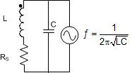 Figure 47. LC Tank
The resistance and inductance of the secondary winding caused by the eddy current can be modeled as a distant dependent resistive and inductive component on the primary side (coil). We can then represent the circuit as an equivalent parallel circuit, as shown in Figure 48.
 Figure 48. Equivalent Parallel Circuit
The value of RP can be calculated with:

where
- RS is the AC series resistance at the frequency of operation.
- C is the parallel capacitance
- L is the inductance
RP can be viewed as the load on the sensor driver; this load corresponds to the current drive needed to maintain the oscillation amplitude. The position of a target can change RP by a significant amount, as shown in Figure 49. The value of RP can then be used to determine the position of a conductive target. If the value of RP is too low, then the sensor driver will not be able to maintain sufficient oscillation amplitude.
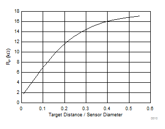 Figure 49. RP vs Target Distance for a 14 mm Diameter Sensor
9.1.2 RP+L Mode Calculations
For many systems which use the LDC1101, the actual sensor RP, sensor frequency, or sensor inductance is not necessary to determine the target position; typically the equation of interest is:
where
- RP_DATA is the contents of registers 0x21 and 0x22
- L_DATA is the contents of registers 0x23 and 0x24
These Position equations are typically system dependent. For applications where the Sensor RP in Ωs needs to be calculated, use Equation 4:

where
- RPDATA is the contents of RP_DATA_MSB and RP_DATA_LSB (registers 0x21 and 0x22),
- RPMIN is the value set by RP_MIN in register RP_SET (register 0x01), and
- RPMAX is the value set by RP_MIN in register RP_SET (register 0x01).
For example, with device settings of:
- RPMIN set to 1.5 kΩ, and
- RPMAX set to 12 kΩ.
If RPDATA = 0x33F1 (register 0x21 = 0xF1 and register 0x22= 0x33), which is 13297 decimal, then the sensor RP = 1.824 kΩ.
If RPMAX_DIS (Register 0x01-b[7]) is set, then the equation is simply:

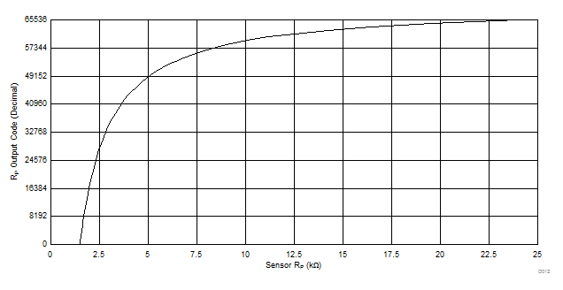 Figure 50. LDC1101 RP Transfer Curve with RPMIN = 1.5 kΩ and RPMAX = 24 kΩ
The sensor frequency in Hz can be calculated from Equation 6:

where
- ƒCLKIN is the frequency input to the CLKIN pin,
- L_DATA is the contents of registers 0x23 and 0x24, and
- RESP_TIME is the programmed response time in register 0x04.
The inductance in Henrys can then be determined from Equation 7:

where
- CSENSOR is the fixed sensor capacitance in Farads, and
- ƒSENSOR is the measured sensor frequency, as calculated in Equation 6 above.
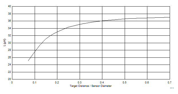 Figure 51. Inductance vs Normalized Target Distance for an Example Sensor
9.1.3 LDC1101 RP Configuration
Setting the RP_MIN and RP_MAX parameters is necessary for proper operation of the LDC1101; the LDC1101 may not be able to effectively drive the sensor with incorrect settings, as the sensor amplitude will be out of the valid operation region. The LDC1101EVM GUI and the LDC Excel® tools spreadsheet (http://www.ti.com/lit/zip/slyc137) can be used to calculate these parameters in an efficient manner.
For RP measurements, the following register settings must be set as follows:
- ALT_CONFIG.LOPTIMAL(register 0x05-bit0) = 0
- D_CONFIG.DOK_REPORT (register 0x0C-bit0) = 0
- Ensure that the sensor characteristics are within the Sensor boundary conditions:
- 500 kHz < ƒSENSOR < 10 MHz
- 100 pF < CSENSOR < 10 nF
- 1 µH < LSENSOR < 500 µH
- Measure the sensor’s resonance impedance with minimal target interaction (RPD∞). The minimal target interaction occurs when the target is farthest away from the sensor for axial sensing solutions or when the target coverage of the sensor is at a minimum for rotational or lateral sensing. Select the appropriate setting for RPMAX (register 0x01-bits [5:4]):
- Measure the sensor’s resonance impedance with the target closest to the sensor (RPD0) as required by the application. Select the largest RPMIN setting that satisfies:
- RPMIN < 0.8 × RPD0
- If the required RPMIN is smaller than 750 Ω, RPD0 must be increased to be compliant with this boundary condition. This can be done by one or more of the following:
- increasing ƒSENSOR
- increasing the minimum distance between the target and the sensor
- reducing the RS of the sensor by use of a thicker trace or wire
- Check if the worst-case Sensor quality factor QMIN=RpMIN × √(CSENSOR/LSENSOR) is within LDC1101’s operating range:
- 10 ≤ QMIN ≤ 400
- If QMIN < 10, for a fixed ƒSENSOR, increase CSENSOR and decrease LSENSOR.
- If QMIN > 400, for a fixed ƒSENSOR, decrease CSENSOR and increse LSENSOR.
- Alternatively the user may choose to not change the current Sensor parameters, but to increase Rp_D0.
RPD∞ ≤ RPMAX ≤ 2RPD∞
If the RP of the sensor is greater than 75 kΩ, RP measurement accuracy may be improved by setting RPMAX_DIS to 1.
9.1.4 Setting Internal Time Constant 1
RP Measurements require configuration of the TC1 and TC2 registers. There are several programmable capacitance and resistance values. Set Time Constant 1 based on minimum sensor frequency:

where
- ƒSENSOR-MIN is the minimum sensor frequency encountered in the system; typically this occurs with no target present.
- VAMP is sensor amplitude of 0.6V,
- R1 is the programmed setting for TC1.R1 (register 0x03-bits[4:0]), and
- C1 is the programmed setting for TC1.C1 (register 0x03-bits[7:6])
The acceptable range of R1 is from 20.6 kΩ to 417.4 kΩ. If several combinations of R1 and C1 are possible, it is recommended to use the largest capacitance setting for C1 that fits the constraints of Equation 8, as this will provide improved noise performance.
9.1.5 Setting Internal Time Constant 2
Set the Time Constant 2 (register 0x03) using Equation 9:
where
- CSENSOR is the parallel capacitance of the sensor.
- RP_MIN is the LDC1101 setting determined in LDC1101 RP Configuration (for example, use 1.5 kΩ when RP_SET.RP_MIN = b110),
- R2 is the programmed setting for TC2.R2 (register 0x03-bits[5:0]), and
- C2 is the programmed setting for TC2.C2 (register 0x03-bits[7:6]).
The acceptable range of R2 is from 24.60 kΩ to 834.8 kΩ. If several combinations of R2 and C2 are possible, it is recommended to program the larger capacitance setting for C2 that fits the constraints of Equation 9, as this will provide improved noise performance.
9.1.6 MIN_FREQ and Watchdog Configuration
The LDC1101 includes a watchdog timer which monitors the sensor oscillation. While in active mode, if no sensor oscillation is detected, the LDC1101 will set STATUS.NO_SENSOR_OSC (register 0x20:bit7), and attempt to restart the oscillator. This restart will reset any active conversion.
The watchdog waits an interval of time based on the setting of DIG_CONF.MIN_FREQ (register 0x04:bits[7:4]). The MIN_FREQ setting is also used to configure the startup of oscillation on the sensor. Select the DIG_CONF.MIN_FREQ (register 0x04-bits[7:4]) setting closest to the minimum sensor frequency; this setting is used for internal watchdog timing. If the watchdog determines the sensor has stopped oscillating, it will report the sensor has stopped oscillating in STATUS. NO_SENSOR_OSC (register 0x20-bit7). If the DIG_CONF.MIN_FREQ is set too low, then the LDC1101 will take a longer time interval to report that the sensor oscillation has stopped.
If the DIG_CONF.MIN_FREQ is set too high, then the watchdog may incorrectly report that the sensor has stopped oscillating and attempt to restart the sensor oscillation.
When the watchdog determines that the sensor has stopped oscillating, the LHR conversion results will contain 0xFFFFFF.
9.1.7 RP+L Sample Rate Configuration with RESP_TIME
The RP+L sample rate can be adjusted by setting by DIG_CONF.RESP_TIME (register 0x04:bits[2:0]). The Response time can be configured from 192 to 6144 cycles of the sensor frequency. Higher values of Response time will have a slower sample rate, but produce a higher resolution conversion.

9.1.8 High Resolution Inductance Calculation (LHR mode)
For many systems which use the LDC1101, the actual sensor frequency or sensor inductance is not necessary to determine the target position. Should the sensor frequency in Hz need to be determined, use Equation 11:

where
- LHRDATA is the contents of registers 0x38, 0x39, and 0x3A,
- LHROFFSET is the programmed contents of registers 0x32 and 0x33,
- SENSOR_DIV is the contents of LHR_CONFIG.SENSOR_DIV (register 0x34-bit[1:0]), and
- ƒCLKIN is the frequency input to the CLKIN pin: ensure that it is within the specified limits of 1 MHz to 16 MHz.
Note that LHR_DATA=0x0000000 indicates a fault condition or that the LDC1101 has never completed an LHR conversion.
The inductance in Henrys can then be determined from the sensor frequency with Equation 12:

where
- CSENSOR is the fixed sensor capacitance, and
- ƒSENSOR is the measured sensor frequency, as calculated above.
Example with the device set to:
- LHR_OFFSET = 0x00FF (register 0x32 = 0xFF, and 0x33 = 0x00)
- ƒCLKIN = 16 MHz
- SENSOR_DIV = b’01 (divide by 2)
and the conversion result is:
LHR_DATA = 0x123456 (register 0x38 = 0x56, register 0x39 = 0x34,register 0x3A = 0x12)
Then entering LHR_DATA = 0x123456 = 1193046 (decimal) into Equation 11:

Results in ƒSENSOR = 2.400066 MHz.
9.1.9 LHR Sample Rate Configuration with RCOUNT
The conversion time represents the number of reference clock cycles used to measure the sensor frequency. The LHR mode conversion time is set by the Reference count in LHR_RCOUNT.RCOUNT (registers 0x30 & 0x31). The LHR conversion time is:

The 55 is due to post-conversion processing and is a fixed value. The reference count value must be chosen to support the required number of effective bits (ENOB). For example, if an ENOB of 13 bits is required, then a minimum conversion time of 213 = 8192 clock cycles is required. 8192 clock cycles correspond to a RCOUNT value of 0x0200.
Higher values for RCOUNT produce higher resolution conversions; the maximum setting, 0xFFFF, is required for full resolution.
9.1.10 Setting RPMIN for LHR Measurements
Configure the RP measurement as shown previously for L measurements. If only L measurements are necessary, then the RP measurement can be disabled by setting:
- ALT_CONFIG.LOPTIMAL(register 0x05-bit0) = 1
- D_CONFIG.DOK_REPORT (register 0x0C-bit0) = 1
Setting these bits disable the sensor modulation used by the LDC1101 to measure RP and can reduce L measurement noise. When the RP modulation is disabled, the LDC1101 will drive a fixed current level into the sensor. The current drive is configured by RP_SET.RPMIN (address 0x01:bits[2:0]). The sensor amplitude must remain between 0.25 Vpk and 1.25 Vpk for accurate L measurements. Use Table 36 to determine the appropriate RPMIN setting, based on the variation in sensor RP. If multiple RPMIN values cover the Sensor RP, use the higher current drive setting. The equation to determine sensor amplitude is:

Table 36. LHR RPMIN Settings when Sensor RP Modulation is Disabled
| RPMIN SETTING | RPMIN FIELD VALUE | SENSOR DRIVE (μA) |
MINIMUM SENSOR RP (kΩ) |
MAXIMUM SENSOR RP (kΩ) |
|---|---|---|---|---|
| 0.75 kΩ | b111 | 600 | 0.53 | 1.65 |
| 1.5 kΩ | b110 | 300 | 1.1 | 3.3 |
| 3 kΩ | b101 | 150 | 2.1 | 6.5 |
| 6 kΩ | b100 | 75 | 4.2 | 13.1 |
| 12 kΩ | b011 | 37.5 | 8.4 | 26.2 |
| 24 kΩ | b010 | 18.7 | 16.9 | 52.4 |
| 48 kΩ | b001 | 9.4 | 33.9 | 105 |
| 96 kΩ | b000 | 4.7 | 67.9 | 209 |
For example, with a sensor that has an RP which can vary between 2.7 kΩ to 5 kΩ, the appropriate setting for RPMIN would be 3 kΩ (RP_SET.RPMIN = b101). For more information on Sensor RP and sensor drive, refer to Configuring Inductive-to-Digital-Converters for Parallel Resistance (RP) Variation in L-C Tank Sensors(SNAA221).
9.1.11 Sensor Input Divider
The reference clock frequency should be greater than 4 times the sensor frequency for optimum measurement resolution:
ƒCLKIN> 4ƒSENSOR-MAX
For higher sensor frequencies, this relationship may not be realizable without the sensor divider. Set the sensor divider to an appropriate value to produce an effective reduction in the sensor frequency:
ƒCLKIN> 4ƒSENSOR-MAX ÷ SENSOR_DIV
9.1.12 Reference Clock Input
Use a clean, low jitter, 40-60% duty cycle clock input with an amplitude swing within the range of VDD and GND; proper clock impedance control, and series or parallel termination is recommended. The rise and fall time should be less than 5 ns. Do not use a spread-spectrum or modulated clock.
For optimum L measurement performance, it is recommended to use the highest reference frequency (16 MHz). LHR conversions will not start until a clock is provided on CLKIN.
9.1.13 INTB Reporting on SDO
INTB is a signal generated by the LDC1101 that reports a change in device status. When INTB_MODE.INTB2SDO=1 (register 0x0A:bit7), INTB is multiplexed onto the SDO pin. Once the reporting is enabled, select the desired signal to report by setting INTB_MODE.INTB_FUNC (register 0x0A:bit[5:0]).
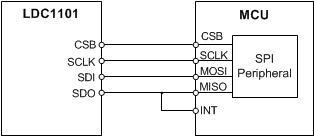 Figure 52. SDO/INTB Connection to MCU
For many microcontrollers, the MISO signal on the SPI peripheral cannot provide the desired interrupt functionality. One method to use the INTB functionality is to connect a second GPIO which triggers on a falling edge, as shown in Figure 51. Table 37 describes the signal functionality that can be programmed onto INTB.
Table 37. INTB Signal Options
| SIGNAL | INTB_FUNC (0x0A:bit[5:0]) |
FUNCTIONALITY | SWITCH OUTPUT TYPE |
|---|---|---|---|
| LHR Data Ready (LHR-DRDY) | b10’0000 | Indicates new High-Resolution Inductance (LHR) conversion data is available. | Latching |
| L_HI_LO | b01’0000 | L Comparator with hysteresis | Hysteresis |
| L_TH_HI | b00’1000 | Latching L High threshold compare | Latching |
| RP+L Data Ready (RPL-DRDY) | b00’0100 | Indicates new RP+L conversion data is available. | Pulse |
| RP_HI_LO | b00’0010 | RP Comparator with hysteresis | Hysteresis |
| RP_TH_HI | b00’0001 | Latching RP High threshold compare | Latching |
| None | b00’0000 | No INTB reporting – SDO pin only provides SDO functionality. | N/A |
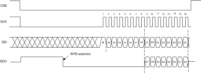 Figure 53. Example INTB Signal on SDO
When INTB_MODE.INTB2SDO (register 0x0A:bit7) = 0, the SDO pin is in a Hi-Z state until the 8th falling edge of SCLK after CSB goes low. When INTB reporting is enabled by setting INTB_MODE.INTB2SDO = 1, after CSB goes low, the SDO pin will go high and remain high until:
- the event configured by INTB_MODE.INTB_FUNC occurs,
- an SPI read transaction is initiated, or
- CSB is deasserted (pulled high)
9.1.14 DRDY (Data Ready) Reporting on SDO
Completion of a conversion can be indicated on the SDO pin by reporting the DRDY signal – there is a conversion complete indicator for the RP+L conversion (RPL-DRDY), and a corresponding conversion complete indicator for the LHR mode (LHR-DRDY).
When LHR-DRDY or RPL-DRDY is reported on SDO, the SDO pin is asserted on completion of a conversion. While in this mode, conversion data can be corrupted if a new conversion completes while reading the output data registers. To avoid data corruption, it is important to retrieve the conversion rates via SPI quicker than the shortest conversion interval, and to ensure that the data is retrieved before a new conversion could possibly complete.
When INTB is reporting RPL-DRDY, if CSB is held low for longer than one conversion cycle, INTB will be deasserted approximately 100 ns to 2 µs prior to the completion of each conversion. The deassertion time is proportional to 1/ƒSENSOR.
When INTB is reporting LHR-DRDY, if CSB is held low for longer than one conversion cycle, INTB will assert on completion of the first conversion and remain low – and it will remain asserted until cleared. To clear the LHR_DRDY signal, read the LHR_DATA registers.
 Figure 54. Reporting RPL-DRDY on INTB/SDO
 Figure 55. Reporting LHR-DRDY on INTB/SDO
Note that the conversion interval for an LHR measurement is asynchronous to the conversion interval for an RP+L measurement, therefore the LHR-DRDY signal cannot be used to determine when to read RP+L conversion results, and vice versa.
9.1.15 Comparator Functionality
The LDC1101 provides comparator functionality, in which the RP+L conversion results can be compared against two thresholds. The results of each RP and L conversion can be compared against programmable thresholds and reported in the STATUS register. Note that the LHR conversion results cannot be used for comparator functionality.
In addition, the INTB signal can be asserted or deasserted when the conversion results increase above a Threshold High or decreases below a Threshold Low registers. In this mode, the LDC1101 essentially behaves as a proximity switch with programmable hysteresis. The threshold HI settings must be programmed to a higher value than the threshold LO registers (for example, if RP_THRESH_LO is set to 0x2000, RP_THRESH_HI should programmed to 0x2001 or higher).
Either Latching and non-latching functions can be reported on INTB/SDO. The INTB signal can report a latching signal or a continuous comparison for each conversion result.
The Threshold setting registers (address 0x06:0x09 and 0x16:0x19) can be changed while the LDC1101 is in active conversion mode. It is recommended to change the register values using an extended SPI transaction as described in SPI Programming, so that the register updates can be completed in a shorter time interval. This functionality enables the LDC1101 to operate as a dynamic tracking switch. LDC1101 output codes can be readout in < 4 μs, and the set of active thresholds can be updated in <6 μs. It is not recommended to update the threshold registers more often than once per conversion interval of the LDC1101 (that is, do not change the threshold register values multiple times in a single conversion interval).
To clear a latched INTB signal, set INTB_MODE = 0x80; it is not necessary for the LDC1101 to be in Sleep mode to clear the latched output; the INTB_MODE can be changed while the LDC1101 is in active mode. After clearing the latched output, re-enabling the INTB_FUNC can be done while in active mode.
Table 38. Comparator Options
| FUNCTION | THRESHOLD HIGH | THRESHOLD LOW | STATUS REPORTING |
INTB/SDO REPORTING |
|---|---|---|---|---|
| RP Comparator with hysteresis | RP_THRESH_HI (registers 0x06 & 0x07) |
RP_THRESH_LO (registers 0x08 & 0x09) |
RP_HI_LON (bit 4) |
RP_HI_LO (INTB_MODE:INTB_FUNC=b00’0010) |
| RP High threshold only (Latching) | RP_THRESH_HI (registers 0x06 & 0x07) |
N/A | RP_HIN (bit 5) |
RP_TH_HI (INTB_MODE:INTB_FUNC=b00’0001) Note that INTB/SDO will latch. |
| L Comparator with hysteresis | L_THRESH_HI (registers 0x16 & 0x17) |
L_THRESH_LO (registers 0x18 & 0x19) |
L_HI_LON (bit 2) |
L_HI_LO (INTB_MODE:INTB_FUNC=b01’0000) |
| L High threshold compare only (Latching) | L_THRESH_HI (registers 0x18 & 0x19) |
N/A | L_HIN (bit 3) | L_TH_HI (INTB_MODE:INTB_FUNC=b00’1000) Note that INTB/SDO will latch. |
space
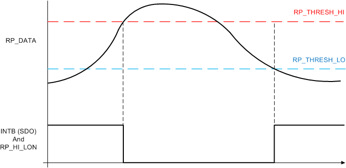 Figure 56. INTB/SDO Output Value for RP Comparator with Hysteresis (INTB_FUNC=b00’0010)
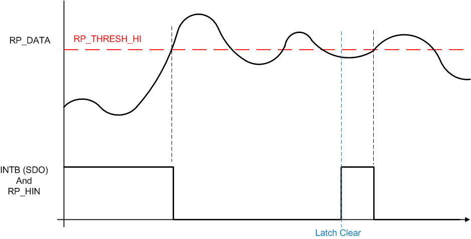 Figure 57. INTB/SDO Output for RP Threshold High (INTB_FUNC=b00’00011)
9.2 Typical Application
Implementation of a system using the LDC1101 first requires determining the appropriate measurement to perform. Refer to http://e2e.ti.com/blogs_/b/analogwire/archive/2015/02/11/inductive-sensing-should-i-measure-l-rp-or-both for guidance.
For systems that require measurement of RP, set the following:
- Configure RP settings as instructed in LDC1101 RP Configuration.
- Set the internal time constants as detailed in Setting Internal Time Constant 1 and Setting Internal Time Constant 2.
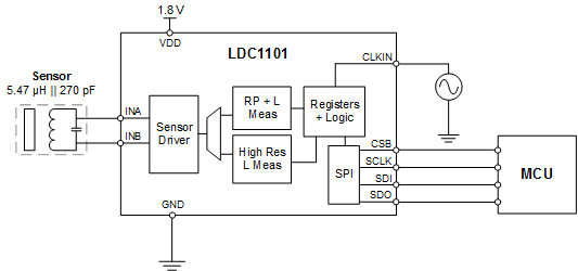 Figure 58. Example LDC1101 Typical Application
9.2.1 Design Requirements
Example of an axial measurement implementation using the LDC1101. In this example, the sensor is an inductor constructed of a multi-layer PCB coil in parallel with a C0G grade surface mount capacitor. For this example, a 10 mm diameter Aluminum target of 1mm thickness is moved perpendicular to the plane of the sensor coil.
For this example, the target range of motion is from 1 mm to 3 mm distance from the sensor coil. The position of the target needs to be reported at a sample rate of 3 ksps. The PCB is a 4-layer construction with 0.1 mm (4 mils) minimum feature size.
9.2.2 Detailed Design Procedure
9.2.2.1 Device Configuration for RP+L Measurement with an Example Sensor
The sensor described in Table 39 meets the restrictions on size on construction. To use it for RP+L measurement of a 10 mm diameter 1 mm thick Aluminum target moving axially with respect to the sensor:
Table 39. Example Sensor Characteristics
| PARAMETER | MINIMUM TARGET INTERACTION | STRONGEST TARGET INTERACTION |
|---|---|---|
| Inductance | 5.47 µH | 5.15 µH |
| Inductor Outer Diameter | 10 mm | |
| Number of Turns | 17 | |
| Trace Spacing/ Trace Width | 0.1 mm / 0.16 mm | |
| Number of Layers/Separation | 2 / 0.355 mm | |
| Sensor Capacitance | 270 pF | |
| Sensor Frequency | 4.11 MHz | 4.27 MHz |
| RS | 3.20 Ω at 2.93 MHz | 3.23 Ω at 4.27 MHz |
| RP | 6.33 kΩ at 2.93 MHz | 5.91 kΩ at 4.27 MHz |
| Q at 2.9 MHz | 45 | 42 |
This sensor is within the LDC1101 sensor boundary conditions for frequency, Q, and RP. The first step is to determine the appropriate RPMIN/RPMAX and TC1/2 settings.
- Setting RPMAX has the constraint of RPD∞ ≤ RpMAX ≤ 2RPD∞
- RPMIN setting using the constraint of RpMIN < 0.8 × RPD0:
- Q Range: In step 4, the sensor Q range of 42 to 45 is within the operating range of 10 to 400. As the sensor Q value is below 50, it is not necessary to use RPMAX_DIS, and so RPMAX_DIS=0.
- Now set the Time Constant 1 using Equation 8:
- Next, set the Time Constant 2 using Equation 9:
- Then configure the MIN_FREQ field. The sensor minimum frequency is 4.11 MHz, which occurs with the minimum target interaction. Therefore, MIN_FREQ is set to 14, which configures the watchdog for 4.0 MHz.
- Next, set the response time. Setting 6144 will provide the highest resolution RP measurement with this sensor. With 6144 the sample rate will be at least 2.01 kSPS. To attain highest resolution with a sample rate of >3 kSPS, the response time setting should be 3072.
- All other device settings can be in their default values.
6.11 kΩ ≤ RPMAX ≤ 12.22 kΩ → Set RPMAX to 12 kΩ
0.8 × 3.20 kΩ = 2.6 kΩ → Set RPMIN to 1.5 kΩ. Therefore, set RPMIN = 1.5 kΩ.
R1 × C1 = 0.75026 ÷ 4.11 MHz = 1.8255E-7s
Starting with the largest C1 value of 6 pF for best noise performance results in R1 = 30.5 kΩ.
This is within the R1 range of 20.6 kΩ to 417.4 kΩ, and so C1 = 6 pF can be used.
Picking the next higher programmable value for R1 → Set R1 = 33.9 kΩ.
R2 × C2 = 2 × 1.5 kΩ × 270 pF = 8.100E-7s
Starting with the largest C2 value of 24 pF (once again, for best noise performance) results in
R2 = 33.75 kΩ.
This is within the programmable R2 value of 24.60 kΩ to 834.8 kΩ, and so 24 pF can be used for C2.
Picking the next higher programmable value for R2 → Set R2 = 43.3 kΩ.
Table 40. LDC1101 Register Settings for RP+L Example Application
| FIELD | FIELD SETTING | FIELD VALUE | REGISTER | REGISTER VALUE |
|---|---|---|---|---|
| RPMAX_DIS | disabled | b0 | RP_SET (0x01) | 0x36 |
| RPMAX | 12.0 kΩ | b011 | ||
| RPMIN | 1.5 kΩ | b110 | ||
| C1 | 6 pF | b11 | TC1 (0x02) | 0xDE |
| R1 | 33.9 kΩ | b1’1110 | ||
| C2 | 24 pF | b11 | TC2 (0x03) | 0xFE |
| R2 | 43.3 kΩ | b11’1110 | ||
| MIN_FREQ | 4.0 MHz | b1110 | DIG_CONF (0x04) | 0xE6 |
| RESP_TIME | 3072 | b110 | ||
| FUNC_MODE | active | b00 | START_CONFIG (0x0B) | 0x00 |
On power-up, the LDC1101 enters Sleep mode, which is a low power mode used to configure the LDC. If the LDC1101 is actively converting, write 0x01 to START_CONFIG (address 0x0B) to stop conversions before writing the settings above.
Once the LDC1101 is configured, the process to retrieve RP+L conversion results is:
- Set the LDC1101 into conversion mode (active mode) by writing 0x00 to START_CONFIG (register 0x0B).
- Poll STATUS.DRDYB (register 0x20:bit6) until it indicates a conversion result is present, or use the INTB signal reporting as described in DRDY (Data Ready) Reporting on SDO.
- If the desired measurement is RP, then read back registers 0x21 and 0x22. The RP output code is the contents of register 0x21 + 256 × (contents of register 0x22).
- If the desired measurement is L, then read back registers 0x23 and 0x24. The L output code is the contents of register 0x23 + 256 × (contents of register 0x24). Reading both RP and L is permitted, for a more efficient operation RP and L registers can be retrieved in a single extended SPI transaction as described in SPI Programming.
- Process the conversion results on the MCU and repeat from step 2 if additional conversions are desired. If no additional conversions are required, place the LDC1101 into Sleep mode or Shutdown mode.
9.2.2.2 Device Configuration for LHR Measurement with an Example Sensor
Given a sensor with characteristics as shown in Table 39, the steps to configure the LDC1101 for LHR measurements are:
- Determine the device sample rate, based on system requirements, using Equation 14. For this example, ƒCLKIN = 16 MHz and a sample rate of 3 kSPS is necessary. The number of cycles of the ƒCLKIN that closest fit the desired sample rate is determined by:
mm 1/(3 kSPS) = 333.3 µs
subtracting the conversion post-processing time of 55 reference clock cycles (55/16 MHz = 3.437 µs):
mm 333.3 µs – 3.437 µs = 329.9 µs → 16 MHz × 163.2 µs = 5278.34 → 5278.34/16 = 329.9
Programming RCOUNT to 330 (0x014A) results in a sample rate of 2.999 kSPS. - Next, set the sensor drive. If the sensor was already configured for RP+L measurements with the steps in Device Configuration for RP+L Measurement with an Example Sensor, then the sensor drive is already configured and no additional steps are necessary.
- If the sensor drive needs to be configured, from Table 36, 3 kΩ is the appropriate setting for the sensor RP range of 6.33 kΩ to 5.61 kΩ.
Table 41. LDC1101 Register Settings for LHR Example Application
| FIELD | FIELD SETTING | FIELD VALUE | REGISTER | REGISTER VALUE |
|---|---|---|---|---|
| RPMAX_DIS | disabled | b0 | RP_SET (0x01) | 0x75 |
| RPMAX | doesn’t matter | b111 | ||
| RPMIN | 1.5 kΩ | b101 | ||
| MIN_FREQ | 4.0 MHz | b1110 | DIG_CONF (0x04) | 0xE7 |
| RESP_TIME | don’t care | b111 | ||
| RCOUNT | 5280 | 330 | LHR_RCOUNT_LSB (0x30) | 0x4A |
| LHR_RCOUNT_MSB (0x31) | 0x01 | |||
| FUNC_MODE | active | b00 | START_CONFIG (0x0B) | 0x00 |
Once the LDC1101 is configured, the process to retrieve LHR conversion results is:
- Set the LDC1101 into conversion mode (active mode) by writing 0x00 to START_CONFIG (register 0x0B).
- Poll LHR_STATUS.DRDYB (register 0x3B:bit0) until it indicates a conversion result is present, or use the INTB signal reporting as described in DRDY (Data Ready) Reporting on SDO.
- Read back registers 0x38, 0x39, and 0x3A. These registers can be retrieved in a single extended SPI transaction as described in SPI Programming.
- Process the conversion results on the MCU and repeat from step 2 if additional conversions are desired. If no additional conversions are required, place the LDC1101 into Sleep mode or Shutdown mode.
Both sets of conversion results can be retrieved when the conversions complete. Note that the RP+L conversions will not complete at the same time as LHR conversions.
9.2.3 Application Curves
The RCOUNT = 0x00FF curve, which corresponds to a sample rate of 3.87 ksps, will measure the target position with a slightly lower resolution than the RCOUNT = 0x014A used in this example. Over the target movement range of 3 mm, which corresponds to the normalized value of 0.3 on the Axial Measurement graph, the target position can be resolved to 4 µm.
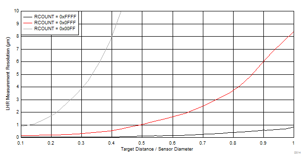 Figure 59. LHR Axial Measurement Resolution vs Normalized Distance for Aluminum Target
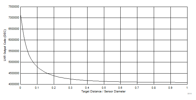 Figure 60. LHR Output Code vs Normalized Distance for Aluminum Target
10 Power Supply Recommendations
A parallel set of 1 µF and 0.1 µF capacitors should be used to bypass VDD, although it may be necessary to include a larger capacitor with systems which have a larger amount of supply variation. The smallest value capacitor should be placed as close as possible to the VDD pin. A ground plane is recommended to connect both the ground and the Die Attach Pad (DAP).
CLDO capacitor should be nonpolarized and have an equivalent series resistance (ESR) less than 1 Ω, with a SRF of at least 24 MHz.
11 Layout
11.1 Layout Guidelines
The LDC1101 requires minimal external components for effective operation. Following good layout techniques - providing good grounding and clean supplies are critical for optimum operation. Due to the small physical size of the LDC1101, use of surface mount 0402 or smaller components can ease routing.
11.1.1 Ground and Power Planes
Ground and power planes are helpful for maintaining a clean supply to the LDC1101. In the layout shown in Figure 61, a top-layer ground fill is also used for improved grounding.
11.1.2 CLKIN Routing
The CLKIN pin routing should maintain consistent impedance; typically this is 50Ω, but can be adjusted based on board geometries. If a parallel termination resistor is used, it should be placed as close as possible to the CLKIN pin. Minimize layer changes and routing through vias for the CLKIN signal. Maintain an uninterrupted ground plane under the trace.
11.1.3 Capacitor Placement
The capacitor CLDO should be placed as close as possible to the CLDO pin.
Place the bypass capacitors as close as possible to the VDD pin, with the smaller valued capacitor placed closer.
11.1.4 Sensor Connections
The sensor capacitor should be as close as possible to the sensor inductor. The INA and INB traces should be routed in parallel and as close as possible to each other to minimize coupling of noise. If cable is to be used, then INA and INB should be a twisted pair or in coaxial cable. The distance between the INA/INB pins and the sensor will affect the maximum possible sensor frequency. For some applications, it may be helpful to place small value capacitor (for example, 10 pF) from INA to ground and INB to ground; these capacitors should be located close to the INA and INB pins.
Refer to Application Note LDC Sensor Design (SNOA930) for additional information on sensor design.
11.2 Layout Example
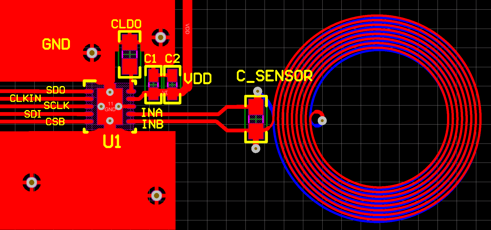 Figure 61. Layout Recommendations