ZHCSD89A October 2014 – January 2015 TPD3S014 , TPD3S044
PRODUCTION DATA.
- 1 特性
- 2 应用
- 3 说明
- 4 简化电路原理图
- 5 修订历史记录
- 6 Device Comparison
- 7 Pin Configuration and Functions
- 8 Specifications
- 9 Detailed Description
- 10Application and Implementation
- 11Power Supply Recommendations
- 12Layout
- 13器件和文档支持
- 14机械封装和可订购信息
12 Layout
12.1 Layout Guidelines
- The optimum placement is as close to the connector as possible.
- EMI during an ESD event can couple from the trace being struck to other nearby unprotected traces, resulting in early system failures.
- The PCB designer needs to minimize the possibility of EMI coupling by keeping any unprotected traces away from the protected traces which are between the TVS and the connector.
- Route the protected traces as straight as possible.
- Eliminate any sharp corners on the protected traces between the TVS and the connector by using rounded corners with the largest radii possible.
- Electric fields tend to build up on corners, increasing EMI coupling.
12.2 Layout Examples
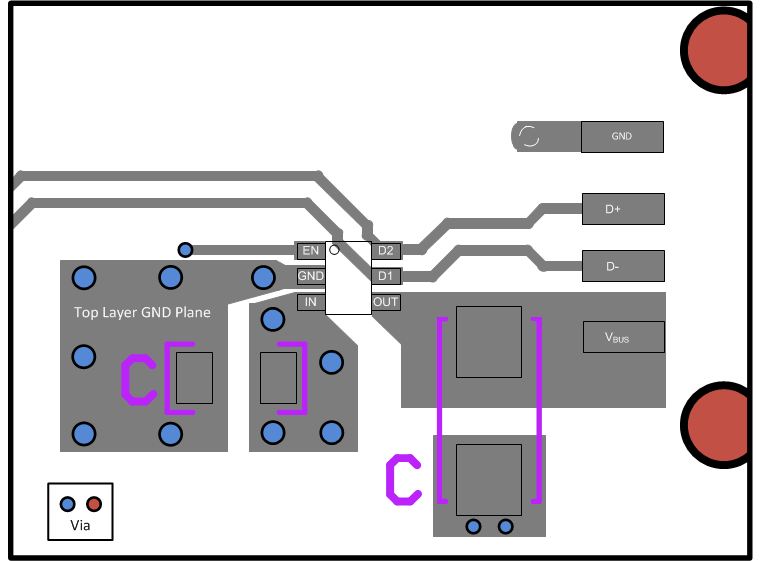
 Figure 37. USB2.0 Type A TPD3S0x4 Board Layout
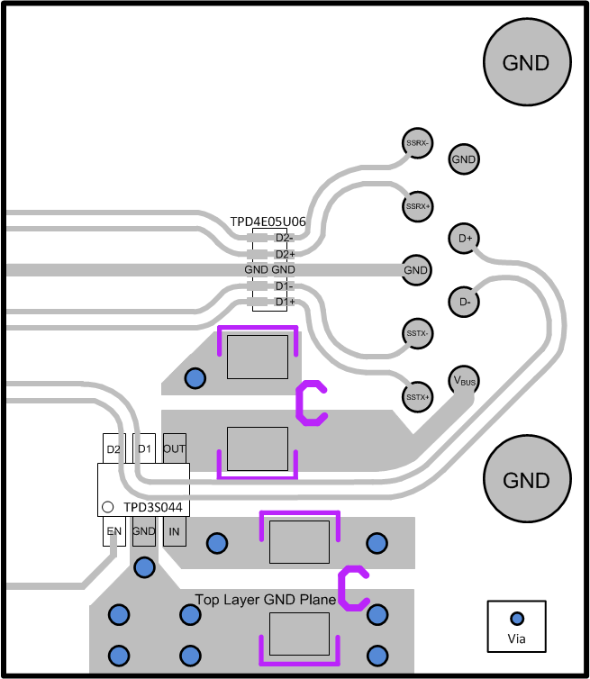
 Figure 38. USB3.0 Type A TPD3S044 Board Layout