ZHCSBA5B June 2013 – September 2014 TPA6133A2
PRODUCTION DATA.
1 特性
2 应用范围
- 移动电话
- 音频耳机
- 笔记本电脑
- 高保真应用
3 说明
TPA6133A2是一款具有 GPIO 控制的立体声 DirectPath™ 头戴式耳机放大器。 TPA6133A2具有最小的静态流耗,IDD的典型值为 4.2mA,这使得它非常适合于便携式应用。 GPIO 控制使得此器件能够被置于低功耗关断模式中。
TPA6133A2是一款信噪比为 93dB 的高保真放大器。 大于 100dB 的 PSRR 可在不影响收听体验的同时实现与电池的直接连接。 12 μVrms 的输出噪声(典型值输入信噪比 (A-weighted))在默声周期期间提供最小的噪声背景。 可配置差分输入和高 CMRR 可在一个移动器件所处的嘈杂环境中实现最大噪声抑制。
- 如需了解所有可用封装,请见数据表末尾的可订购产品附录。
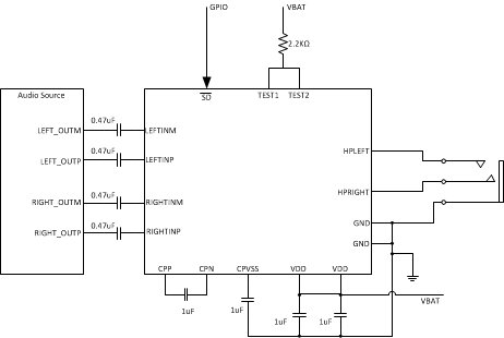
4 简化应用示意图