• Menu
  • Product
  • Email
  • PDF
  • Order now
  • TPS7A8300 2A,6µVRMS,射频 (RF),低压降 (LDO) 稳压器

    • ZHCSBA4E May   2013  – August 2014 TPS7A8300

      PRODUCTION DATA.  

  • CONTENTS
  • SEARCH
  • TPS7A8300 2A,6µVRMS,射频 (RF),低压降 (LDO) 稳压器
  1. 1 特性
  2. 2 应用范围
  3. 3 说明
  4. 4 修订历史记录
  5. 5 Pin Configurations and Functions
  6. 6 Specifications
    1. 6.1 Absolute Maximum Ratings
    2. 6.2 Handling Ratings
    3. 6.3 Recommended Operating Conditions
    4. 6.4 Thermal Information
    5. 6.5 Electrical Characteristics
    6. 6.6 Typical Characteristics
  7. 7 Detailed Description
    1. 7.1 Overview
    2. 7.2 Functional Block Diagram
    3. 7.3 Feature Description
      1. 7.3.1 ANY-OUT Programmable Output Voltage
      2. 7.3.2 Adjustable Operation
      3. 7.3.3 ANY-OUT Operation
      4. 7.3.4 2-A LDO with an Internal Charge Pump
        1. 7.3.4.1 Dropout Voltage (VDO)
        2. 7.3.4.2 Output Voltage Accuracy
        3. 7.3.4.3 Internal Charge Pump
      5. 7.3.5 Low-Noise, 0.8-V Reference
      6. 7.3.6 Internal Protection Circuitry
        1. 7.3.6.1 Undervoltage Lockout (UVLO)
        2. 7.3.6.2 Internal Current Limit (I(LIM))
        3. 7.3.6.3 Thermal Protection
      7. 7.3.7 Programmable Soft-Start
      8. 7.3.8 Power-Good Function
      9. 7.3.9 Integrated Resistance Network (ANY-OUT)
    4. 7.4 Device Functional Modes
      1. 7.4.1 Operation with 1.1 V > VIN > 1.4 V
      2. 7.4.2 Operation with 1.4 V ≥ VIN > 6.5 V
      3. 7.4.3 Disabled
  8. 8 Application and Implementation
    1. 8.1 Application Information
      1. 8.1.1 Start-Up
        1. 8.1.1.1 Enable (EN) and Undervoltage Lockout (UVLO)
        2. 8.1.1.2 Noise-Reduction and Soft-Start Capacitor (CNR/SS)
        3. 8.1.1.3 Soft-Start and Inrush Current
      2. 8.1.2 Capacitor Recommendation
        1. 8.1.2.1 Input and Output Capacitor Requirements (CIN and COUT)
        2. 8.1.2.2 Feed-Forward Capacitor (CFF)
      3. 8.1.3 AC Performance
        1. 8.1.3.1 Power-Supply Ripple Rejection (PSRR)
        2. 8.1.3.2 Load-Step Transient Response
        3. 8.1.3.3 Noise
        4. 8.1.3.4 Behavior when Transitioning from Steady Dropout into Regulation
      4. 8.1.4 Power Dissipation (PD)
      5. 8.1.5 Estimating Junction Temperature
    2. 8.2 Typical Application
      1. 8.2.1 Design Requirements
      2. 8.2.2 Detailed Design Procedure
      3. 8.2.3 Application Curves
    3. 8.3 Do's and Don'ts
  9. 9 Power-Supply Recommendations
  10. 10Layout
    1. 10.1 Layout Guidelines
      1. 10.1.1 Board Layout
    2. 10.2 Layout Example
  11. 11器件和文档支持
    1. 11.1 器件支持
      1. 11.1.1 开发支持
        1. 11.1.1.1 评估模块
        2. 11.1.1.2 Spice 模型
      2. 11.1.2 器件命名规则
    2. 11.2 文档支持
      1. 11.2.1 相关文档 
    3. 11.3 Trademarks
    4. 11.4 Electrostatic Discharge Caution
    5. 11.5 术语表
  12. 12机械封装和可订购信息
  13. 重要声明
search No matches found.
  • Full reading width
    • Full reading width
    • Comfortable reading width
    • Expanded reading width
  • Card for each section
  • Card with all content


DATA SHEET

TPS7A8300 2A,6µVRMS,射频 (RF),低压降 (LDO) 稳压器

本资源的原文使用英文撰写。 为方便起见,TI 提供了译文;由于翻译过程中可能使用了自动化工具,TI 不保证译文的准确性。 为确认准确性,请务必访问 ti.com 参考最新的英文版本(控制文档)。

1 特性

  • 超低压降: 2A 时的最大值为 125mV
  • 输出电压噪声:6µVRMS
  • 电源纹波抑制:
    • 在 1MHz 时为 40dB
  • 输入电压范围:
    • 无偏置:1.4V 至 6.5V
    • 有偏置:1.1V 至 6.5V
  • 两个输出电压模式:
    • ANY-OUT™ 版本(借助印刷电路板 (PCB) 布局布线的用户可调输出):
      • 无需外部电阻
      • 输出电压范围:0.8V 至 3.95V
    • 可调版本:
      • 输出电压范围:0.8V 至 5.0V
  • 线路、负载和温度上精度 1.0%
  • 与 22µF 陶瓷电容器一起工作时保持稳定
  • 可编程软启动输出
  • 电源正常 (PG) 输出
  • 提供的封装:
    • 5mm × 5mm VQFN-20
    • 3.5mm × 3.5mm VQFN-20

2 应用范围

  • 射频 (RF),IF 组件:压控振荡器 (VCO),数模转换器 (ADC),模数转换器 (DAC),低压差分信令 (LVDS)
  • 无线基础设施:串化解串器 (SerDes),现场可编程栅极阵列 (FPGA), DSP™
  • 测试和测量
  • 仪器仪表、医疗和音频
alt_sbvs197.gif

3 说明

TPS7A8300 是一款低噪声 (6µVRMS),低压降 (LDO) 稳压器,能够在压降最大值只有 125mV 的情况下提供一个 2A 负载。

用户完全可以通过印刷电路板 (PCB) 布局布线来调节 TPS7A8300 输出电压,而无需外部电阻器,从而减少元件总数量。 对于更高输出电压应用,此器件在使用外部电阻器的情况下可实现高达 5V 的输出电压。 借助于一个额外的偏置电压轨,此器件支持极低输出电压(低至 1.1V)。

借助于极高精度(线路、负载和温度范围内达到 1%),遥感和可以减少涌入电流的软启动功能,TPS7A8300 非常适合为诸如高端微处理器和现场可编程门阵列 (FPGA) 等高电流、低电压的器件供电。

TPS7A8300 针对高速通信应用中的加电噪声敏感组件而设计。 极低噪声,6-µVRMS器件输出和高宽带电源抑制比 (PSRR)(1MHz 时为
40dB)大大减少了高频信号中的相位噪声和时钟抖动。 这些特性大大增加了计时器件、模数转换器 (ADC) 和数模转换器 (DAC) 的性能。

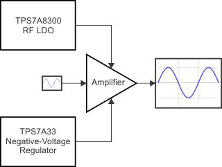
对于需要正向和负向低噪声电源轨的应用,请考虑 TI 的TPS7A33负向高电压、超低噪声线性稳压器系列产品。

器件信息(1)

部件号 封装 封装尺寸(标称值)
TPS7A8300 超薄四方扁平无引线封装 (VQFN) (20) 5.00mm x 5.00mm
超薄四方扁平无引线封装 (VQFN) (20) 3.50mm x 3.50mm
  1. 如需了解所有可用封装,请见数据表末尾的可订购产品附录。

4 修订历史记录

Changes from D Revision (February 2013) to E Revision

  • 更改了格式以满足最新数据表标准;添加了新的部分并移动了现有部分Go
  • 更改了第五个特性要点下的第一个分项 ANY-OUTGo
  • 更改了第八个特性要点:将软启动输出和 PG 输出拆成了两个单独的特性要点Go
  • 更改了说明部分中第二段的第一句。Go
  • Changed RGW and RGR drawings: removed spacing between number and unit in pins 5 to 7 and 9 to 11 Go
  • Changed first row of Pin Functions table: deleted spacing between number and unit in pin namesGo
  • Added capacitor value to BIAS pin description in Pin Functions tableGo
  • Changed 87% to 89% in the PG pin description of the Pin Functions tableGo
  • Changed thermal pad description in Pin Functions tableGo
  • Changed conditions statements for Absolute Maximum Ratings and Recommended Operating Conditions tables Go
  • Added Recommended Operating Conditions tableGo
  • Changed the Typical Characteristics section: changed all curve titles and conditions Go
  • Changed title of Figure 11Go
  • Added Overview section Go
  • Changed second paragraph of Overview section: changed that can be groups, as follows to includingGo
  • Changed functional block diagram footnoteGo
  • Added Feature Description sectionGo
  • Changed adjustable version to adjustable configuration in first paragraph of Adjustable Operation section Go
  • Changed Figure 51: removed right-hand side diagramGo
  • Added Figure 52Go
  • Changed second sentence in Internal Charge Pump section Go
  • Changed last sentence of UVLO sectionGo
  • Changed oscillates to cycles in first paragraph of Thermal Protection sectionGo
  • Changed first sentence of Programmable Soft-Start sectionGo
  • Added Device Functional Modes sectionGo
  • Added Application Information section Go
  • Changed second paragraph of Noise sectionGo
  • Added Typical Application section Go
  • Added Figure 57Go

Changes from C Revision (July 2013) to D Revision

  • Changed 将文档状态从混合状态更改为生产数据Go
  • Deleted 删除了最后一个特性要点中第二个分项的脚注Go
  • Deleted footnote from RGR package drawingGo
  • Changed GND pin description in Pin Descriptions tableGo

Changes from B Revision (July 2013) to C Revision

  • Deleted PG Functionality sectionGo
  • Changed Power-Good sectionGo
  • Changed text in Feed-Forward Capacitor subsectionGo

Changes from A Revision (June 2013) to B Revision

  • 从产品预览更改为生产数据(混合状态)Go

Changes from * Revision (May 2013) to A Revision

  • 更改了产品预览数据表Go

5 Pin Configurations and Functions

RGW Package
5-mm × 5-mm VQFN-20
(Top View)
po_bvs197.gif
RGR Package
3.5-mm × 3.5-mm VQFN-20
(Top View)
po_bvs197.gif

Pin Functions

PIN DESCRIPTION
NAME NO. I/O
50mV, 100mV, 200mV, 400mV, 800mV, 1.6V 5, 6, 7, 9, 10, 11 I Output voltage setting pins. These pins should be connected to ground or left floating. Connecting these pins to ground increases the output voltage by the value of the pin name; multiple pins can be simultaneously connected to GND to select the desired output voltage. Leave these pins floating (open) when not in use. See the ANY-OUT Programmable Output Voltage section for more details.
BIAS 12 I BIAS supply voltage pin for the use of 1.1 V ≤ VIN ≤ 1.4 V and to connect a 10-µF capacitor between this pin and ground.
EN 14 I Enable pin. Driving this pin to logic high enables the device; driving this pin to logic low disables the device. See the Start-Up section for more details.
FB 3 I Output voltage feedback pin connected to the error amplifier. Although not required, a 10-nF feed-forward capacitor from FB to OUT (as close to the device as possible) is recommended for low-noise applications to maximize ac performance. The use of a feed-forward capacitor may disrupt PG (power good) functionality. See the ANY-OUT Programmable Output Voltage and Adjustable Operation sections for more details.
GND 8, 18 — Ground pin. These pins must be externally shorted for the RGR package option.
IN 15-17 I Input supply voltage pin. A 10-μF input ceramic capacitor is required. See the Input and Output Capacitor Requirements (CIN and COUT) section for more details.
OUT 1, 19, 20 O Regulated output pin. A 22-μF or larger ceramic capacitor is required for stability (a 10-μF minimum effective capacitance is required). See the Input and Output Capacitor Requirements (CIN and COUT) section for more details.
PG 4 O Active-high power-good pin. An open-drain output indicates when the output voltage reaches 89% of the target. The use of a feed-forward capacitor may disrupt PG (power good) functionality. See the Power-Good Function section for more details.
SNS 2 I Output voltage sense input pin. Connect this pin only if the ANY-OUT feature is used. See the ANY-OUT Programmable Output Voltage and Adjustable Operation sections for more details.
NR/SS 13 — Noise-reduction and soft-start pin. Connecting an external capacitor between this pin and ground reduces reference voltage noise and also enables the soft-start function. Although not required, a capacitor is recommended for low-noise applications to connect a 10-nF capacitor from NR/SS to GND (as close to the device as possible) to maximize ac performance. See the Noise-Reduction and Soft-Start Capacitor (CNR/SS) section for more details.
Thermal Pad Pad — Connect the thermal pad to a large-area ground plane. The thermal pad is internally connected to GND.

6 Specifications

6.1 Absolute Maximum Ratings

over junction temperature range (unless otherwise noted)(1)
MIN MAX UNIT
Voltage IN, BIAS, PG, EN –0.3 7.0 V
IN, BIAS, PG, EN (5% duty cycle) –0.3 7.5 V
SNS, OUT –0.3 VIN + 0.3(2) V
NR/SS, FB –0.3 3.6 V
50mV, 100mV, 200mV, 400mV, 800mV, 1.6V –0.3 VOUT + 0.3 V
Current OUT Internally limited A
PG (sink current into device) 5 mA
Operating junction temperature, TJ –55 150 °C
(1) Stresses beyond those listed under Absolute Maximum Ratings may cause permanent damage to the device. These are stress ratings only, which do not imply functional operation of the device at these or any other conditions beyond those indicated under Recommended Operating Conditions. Exposure to absolute-maximum-rated conditions for extended periods may affect device reliability.
(2) The absolute maximum rating is VIN + 0.3 V or 7.0 V, whichever is smaller.

6.2 Handling Ratings

MIN MAX UNIT
Tstg Storage temperature range –55 150 °C
V(ESD) Electrostatic discharge Human body model (HBM), per ANSI/ESDA/JEDEC JS-001, all pins(1) –2 2 kV
Charged device model (CDM), per JEDEC specification JESD22-C101, all pins(2) –500 500 V
(1) JEDEC document JEP155 states that 500-V HBM allows safe manufacturing with a standard ESD control process.
(2) JEDEC document JEP157 states that 250-V CDM allows safe manufacturing with a standard ESD control process.

6.3 Recommended Operating Conditions

over junction temperature range (unless otherwise noted)
MIN MAX UNIT
VIN Input supply voltage range 1.1 6.5 V
VBIAS Bias supply voltage range(1) 3.0 6.5 V
IOUT Output current 0 2 A
TJ Operating junction temperature –40 125 °C

6.4 Thermal Information

THERMAL METRIC(1) TPS7A8300 UNIT
RGW (QFN) RGR (QFN)
20 PINS 20 PINS
RθJA Junction-to-ambient thermal resistance 33.6 35.4 °C/W
RθJC(top) Junction-to-case (top) thermal resistance 30.0 47.6
RθJB Junction-to-board thermal resistance 14.0 12.3
ψJT Junction-to-top characterization parameter 0.2 0.5
ψJB Junction-to-board characterization parameter 14.0 12.4
RθJC(bot) Junction-to-case (bottom) thermal resistance 1.6 1.0
(1) For more information about traditional and new thermal metrics, see the IC Package Thermal Metrics application report, SPRA953.

6.5 Electrical Characteristics

Over operating temperature range (TJ = –40°C to 125°C), {1.1 V ≤ VIN < 1.4 V and 3.0 V ≤ VBIAS ≤ 6.5 V} or {VIN ≥ 1.4 V and VBIAS open}(1), VIN ≥ VOUT(TARGET) + 0.3 V(2), VOUT(TARGET) = 0.8 V, OUT connected to 50 Ω to GND(3), VEN = 1.1 V, COUT =
22 μF, CNR/SS = 0 nF, CFF = 0 nF, and PG pin pulled up to VIN with 100 kΩ, unless otherwise noted.
Typical values are at TJ = 25°C.
PARAMETER TEST CONDITIONS MIN TYP MAX UNIT
VIN Input supply voltage range 1.1 6.5 V
VBIAS Bias supply voltage range(1) 3.0 6.5 V
V(REF) Reference voltage V(REF) = V(FB) = V(NR/SS) 0.8 V
VUVLO1(IN) Input supply UVLO with BIAS VIN increasing 1.02 1.085 V
VHYS1(IN) VUVLO1(IN) hysteresis 320 mV
VUVLO2(IN) Input supply UVLO without BIAS VIN increasing 1.31 1.39 V
VHYS2(IN) VUVLO2(IN) hysteresis 253 mV
VUVLO(BIAS) Bias supply UVLO VBIAS increasing 2.83 2.9 V
VHYS(BIAS) VUVLO(BIAS) hysteresis 290 mV
VOUT Output voltage range Using voltage setting pins (50mV, 100mV, 200mV, 400mV, 800mV, and 1.6V) 0.8 – 1.0% 3.95 + 1.0% V
Using external resistors 0.8 – 1.0% 5.0 + 1.0% V
Output voltage accuracy(4)(5) 0.8 V ≤ VOUT ≤ 5 V, 5 mA ≤ IOUT ≤ 2 A –1.0% 1.0%
VIN = 1.5 V, VOUT = 1.2 V, 5 mA ≤ IOUT ≤ 1.2 A –1.0% 1.0%
ΔVO(ΔVI) Line regulation IOUT = 5 mA, 1.4 V ≤ VIN ≤ 6.5 V 0.003 %/V
ΔVO(ΔIO) Load regulation 5 mA ≤ IOUT ≤ 2 A 0.0001 %/A
V(DO) Dropout voltage VIN ≥ 1.4 V and VBIAS open, 0.8 V ≤ VOUT ≤ 5.0 V,
IOUT = 2 A, VFB = 0.8 V – 3%
200 mV
VIN = 1.1 V, VBIAS = 5.0 V,
VOUT(TARGET) = 0.8 V, IOUT = 2 A, VFB = 0.8 V – 3%
125 mV
I(LIM) Output current limit VOUT forced at 0.9 × VOUT(TARGET),
VIN = VOUT(TARGET) + 300 mV
2.1 3.4 4.2 A
I(GND) GND pin current Minimum load,
VIN = 6.5 V, no VBIAS supply, IOUT = 5 mA
2.8 4 mA
Maximum load,
VIN = 1.4 V, no VBIAS supply, IOUT = 2 A
3.7 5 mA
Shutdown, PG = (open),
VIN = 6.5 V, no VBIAS supply, V(EN) = 0.5 V
2.5 μA
I(EN) EN pin current VIN = 6.5 V, no VBIAS supply, V(EN) = 0 V and 6.5 V –0.1 0.1 μA
I(BIAS) BIAS pin current VIN = 1.1 V, VBIAS = 6.5 V,
VOUT(TARGET) = 0.8 V, IOUT = 2 A
2.3 3.5 mA
VIL(EN) EN pin low-level input voltage (disable device) 0 0.5 V
VIH(EN) EN pin high-level input voltage (enable device) 1.1 6.5 V
VIT(PG) PG pin threshold For the direction PG↓ with decreasing VOUT 0.82 VOUT 0.872 VOUT 0.93 VOUT V
Vhys(PG) PG pin hysteresis For PG↑ 0.02 VOUT V
VOL(PG) PG pin low-level output voltage VOUT < VIT(PG), IPG = –1 mA (current into device) 0.4 V
Ilkg(PG) PG pin leakage current VOUT > VIT(PG), V(PG) = 6.5 V 1 μA
I(NR/SS) NR/SS pin charging current VNR/SS = GND, VIN = 6.5 V 4.0 6.2 9.0 μA
IFB FB pin leakage current VIN = 6.5 V –100 100 nA
PSRR Power-supply ripple rejection f = 1 MHz, VIN = 3.8 V, VOUT = 3.3 V, IOUT = 2 A,
CNR/SS = 10 nF, CFF = 10 nF
40 dB
Vn Output noise voltage BW = 10 Hz to 100 kHz, VIN = 1.4 V, VOUT = 0.8 V,
IOUT = 1.5 A, CNR/SS = 10 nF, CFF = 10 nF
6 μVRMS
Tsd Thermal shutdown temperature Shutdown, temperature increasing 160 °C
Reset, temperature decreasing 140 °C
TJ Operating junction temperature –40 125 °C
(1) BIAS supply is required when the VIN supply is below 1.4 V. Conversely, no BIAS supply is needed when the VIN supply is higher than or equal to 1.4 V.
(2) VOUT(TARGET) is the calculated VOUT target value from the output voltage setting pins: 50mV, 100mV, 200mV, 400mV, 800mV, and 1.6V in a fixed configuration. In an adjustable configuration, VOUT(TARGET) is the expected VOUT value set by the external feedback resistors.
(3) This 50-Ω load is disconnected when the test conditions specify an IOUT value.
(4) When the device is connected to external feedback resistors at the FB pin, external resistor tolerances are not included.
(5) The device is not tested under conditions where VIN > VOUT + 2.5 V and IOUT = 2 A, because the power dissipation is higher than the maximum rating of the package. Also, this accuracy specification does not apply on any application condition that exceeds the power dissipation limit of the package under test.

6.6 Typical Characteristics

At TJ = 25°C, {1.1 V ≤ VIN < 1.4 V and 3.0 V ≤ VBIAS ≤ 6.5 V} or {VIN ≥ 1.4 V and VBIAS open}
(1) BIAS supply is required when the VIN supply is below 1.4 V. Conversely, no BIAS supply is needed when the VIN supply is higher than or equal to 1.4 V.
, VIN ≥ VOUT(TARGET) + 0.3 V, VOUT(TARGET) = 0.8 V, OUT connected to 50 Ω to GND, VEN = 1.1 V, COUT = 22 μF, CNR/SS = 0 nF, CFF = 10 nF, and PG pin pulled up to VIN with 100 kΩ, unless otherwise noted.
C001_SBVS197.png
VOUT(TARGET) = 0.8 V, IOUT = 5 mA, VBIAS = Open
Figure 1. Minimum ANY-OUT VOUT Line Regulation
C003_SBVS197.png
VOUT(TARGET) = 0.8 V, VIN = 1.4 V, VBIAS = Open
Figure 3. Minimum ANY-OUT VOUT, Minimum VIN, No BIAS Load Regulation
C005_SBVS197.png
VOUT(TARGET) = 0.8 V, VIN = 1.1 V, IOUT = 5 mA
Figure 5. Minimum ANY-OUT VOUT, Minimum VIN BIAS
Line Regulation
C007_SBVS197.png
VOUT(TARGET) = 0.8 V, VIN = 1.1 V, VBIAS = 6.5 V
Figure 7. Minimum Adjustable VOUT, Minimum VIN,
Maximum BIAS Load Regulation
C009_SBVS197.png
VOUT(TARGET) = 5 V, IOUT = 5 mA, VBIAS = Open
Figure 9. Maximum Adjustable VOUT, No BIAS
Line Regulation
C011_SBVS197.png
VOUT(TARGET) = 5 V, VIN = 5.3 V, VBIAS = Open
Figure 11. Maximum Adjustable VOUT Load Regulation
C013_SBVS197.png
VIN = 5.5 V, ANY-OUT, VBIAS = Open,
Figure 13. Dropout Voltage vs Output Current
C015_SBVS197.png
VBIAS = Open, IOUT = 2 A, ANY-OUT
Figure 15. Dropout Voltage vs Input Voltage
C017_SBVS197.png
VIN = 1.1 V, ANY-OUT, IOUT = 2 A
Figure 17. Minimum VIN Dropout Voltage vs Bias Voltage
C019_SBVS197.png
VOUT(TARGET) = 0.8 V, IOUT = 5 mA, VIN = 1.1 V
Figure 19. Minimum ANY-OUT VOUT, Minimum VIN
Quiescent Current vs Bias Voltage
C021_SBVS197.png
VOUT(TARGET) = 0.8 V, VIN = 1.1 V, VBIAS = 3 V
Figure 21. Minimum ANY-OUT VOUT, VIN, and BIAS
Quiescent Current vs Output Current
C023_SBVS197.png
VOUT(TARGET) = 0.8 V, VIN = 1.1 V
Figure 23. Minimum ANY-OUT VOUT, Minimum VIN
Shutdown Current vs Bias Voltage
C025_SBVS197.png
VIN = 1.8 V, ANY-OUT, VBIAS = Open, VOUT(TARGET) = 1.5 V
Figure 25. Current Limit vs Output Voltage
C027_SBVS197.png
VOUT(TARGET) = 0.8 V, VIN = 1.1 V, VBIAS = 3 V
Figure 27. Minimum ANY-OUT VOUT, VIN, and BIAS
Current Limit vs Output Voltage
C029_SBVS197.png
VOUT(TARGET) = 0.8 V, VBIAS = 3.0 V
Figure 29. Minimum ANY-OUT VOUT, Minimum BIAS
Input UVLO Threshold vs Temperature
C031_SBVS197.png
VOUT(TARGET) = 0.8 V, VIN = 1.1 V
Figure 31. Minimum ANY-OUT VOUT, Minimum VIN BIAS
UVLO Threshold vs Temperature
C033_SBVS197.png
VOUT(TARGET) = 0.8 V, VIN = 6.5 V, VBIAS = Open
Figure 33. Minimum ANY-OUT VOUT, Maximum VIN
Enable Threshold vs Temperature
C035_SBVS197.png
VIN = 6.5 V, VOUT(TARGET) = 0.8 V, VBIAS = Open
Figure 35. Minimum ANY-OUT VOUT, Maximum VIN, No BIAS PG Low Voltage vs PG Current
C037_SBVS197.png
VOUT(TARGET) = 0.8 V, VIN = 6.5 V, VBIAS = Open
Figure 37. Minimum ANY-OUT VOUT, Maximum VIN
PG Threshold vs Temperature
C039_SBVS197.png
VOUT(TARGET) = 0.8 V, VIN = VPG = 6.5 V, VBIAS = Open
Figure 39. Minimum ANY-OUT VOUT, Maximum VIN
PG Current vs Temperature
C041_SBVS197.png
VOUT(TARGET) = 3.3 V, ANY-OUT, VIN = VEN = 3.8 V, VBIAS = Open, IOUT = 1.5 A, COUT = 22 µF, CFF = 10 nF
Figure 41. Power-Supply Rejection vs CNR/SS
C043_SBVS197.png
VIN = VOUT(TARGET) + 0.5 V, ANY-OUT, VBIAS = Open, IOUT = 1.5 A, COUT = 22 µF, CNR/SS = CFF = 10 nF
Figure 43. Spectral Noise Density vs Output Voltage
C045_SBVS197.png
VIN = 3.8 V, VOUT(TARGET) = 3.3 V, ANY-OUT, VBIAS = Open,
IOUT = 1.5 A, COUT = 22 µF, CNR/SS = 10 nF
Figure 45. Spectral Noise Density vs CFF
start_up_Cnr_0nF_SBVS197.gif
VIN = 1.4 V, VOUT = 0.8 V, CNR/SS = 0 nF
Figure 47. Start-Up (CNR/SS = 0 nF)
line_tran_SBVS197.gif
VIN = 1.4 V to 6 V to 1.4 V at 1 V/µs,
VOUT = 0.8 V, IOUT = 2 A, CNR/SS = CFF = 10 nF
Figure 49. Line Transient
C002_SBVS197.png
VOUT(TARGET) = 3.95 V, IOUT = 5 mA, VBIAS = Open
Figure 2. Maximum ANY-OUT VOUT Line Regulation
C004_SBVS197.png
VOUT(TARGET) = 3.95 V, VIN = 4.25 V, VBIAS = Open
Figure 4. Maximum ANY-OUT VOUT Load Regulation
C006_SBVS197.png
VOUT(TARGET) = 0.8 V, VIN = 1.1 V, VBIAS = 3 V
Figure 6. Minimum ANY-OUT VOUT, VIN, and BIAS
Load Regulation
C008_SBVS197.png
VOUT(TARGET) = 0.8 V, IOUT = 5 mA, VBIAS = Open
Figure 8. Minimum Adjustable VOUT, No BIAS
Line Regulation
C010_SBVS197.png
VOUT(TARGET) = 0.8 V, VIN = 1.4 V, VBIAS = Open
Figure 10. Minimum Adjustable VOUT, Minimum VIN,
No BIAS Load Regulation
C012_SBVS197.png
VIN = 1.4 V, ANY-OUT, VBIAS = Open, No BIAS
Figure 12. Minimum VIN Dropout Voltage vs Output Current
C014_SBVS197.png
VBIAS = Open, IOUT = 0.5 A, ANY-OUT
Figure 14. Dropout Voltage vs Input Voltage
C016_SBVS197.png
VIN = 1.1 V, ANY-OUT, IOUT = 0.5 A
Figure 16. Dropout Voltage vs Bias Voltage
C018_SBVS197.png
VOUT(TARGET) = 0.8 V, IOUT = 5 mA, VBIAS = Open
Figure 18. Minimum ANY-OUT VOUT, No BIAS
Quiescent Current vs Input Voltage
C020_SBVS197.png
VOUT(TARGET) = 0.8 V, VIN = 1.4 V, VBIAS = Open
Figure 20. Minimum ANY-OUT VOUT, Minimum VIN, No BIAS Quiescent Current vs Output Current
C022_SBVS197.png
VOUT(TARGET) = 0.8 V, VBIAS = Open
Figure 22. Minimum ANY-OUT VOUT, No BIAS
Shutdown Current vs Input Voltage
C024_SBVS197.png
VOUT(TARGET) = 0.8 V, VBIAS = Open
Figure 24. Minimum ANY-OUT VOUT, No BIAS
Soft-Start Current vs Input Voltage
C026_SBVS197.png
VOUT(TARGET) = 3.95 V, VIN = 4.25 V, VBIAS = Open
Figure 26. Maximum ANY-OUT VOUT
Current Limit vs Output Voltage
C028_SBVS197.png
VOUT(TARGET) = 0.8 V, VIN = 1.1 V, VBIAS = 6.5 V
Figure 28. Minimum ANY-OUT VOUT, Minimum VIN,
Maximum BIAS Current Limit vs Output Voltage
C030_SBVS197.png
VOUT(TARGET) = 0.8 V, VBIAS = Open
Figure 30. Minimum ANY-OUT VOUT, No BIAS
Input UVLO Threshold vs Temperature
C032_SBVS197.png
VOUT(TARGET) = 0.8 V, VIN = 1.4 V, VBIAS = Open
Figure 32. Minimum ANY-OUT VOUT, Minimum VIN, No BIAS Enable Threshold vs Temperature
C034_SBVS197.png
VOUT(TARGET) = 0.8 V, VIN = VEN = 6.5 V, VBIAS = Open
Figure 34. Minimum ANY-OUT VOUT, Maximum VIN
Enable Current vs Temperature
C036_SBVS197.png
VOUT(TARGET) = 0.8 V, VIN = 1.4 V, VBIAS = Open
Figure 36. Minimum ANY-OUT VOUT, Minimum VIN, No BIAS PG Low Voltage vs PG Current
C038_SBVS197.png
VOUT(TARGET) = 0.8 V, VIN = 1.4 V, VBIAS = Open
Figure 38. Minimum ANY-OUT VOUT, Maximum VIN, No BIAS PG Threshold vs Temperature
C040_SBVS197.png
VOUT(TARGET) = 3.3 V, ANY-OUT, VIN = VEN = 3.8 V, VBIAS = Open, COUT = 22 µF, CNR/SS = CFF = 10 nF
Figure 40. Power-Supply Rejection vs Output Current
C042_SBVS197.png
VOUT(TARGET) = 1.2 V, ANY-OUT, VBIAS = Open, IOUT = 1.5 A, COUT = 22 µF, CNR/SS = CFF = 10 nF
Figure 42. Power-Supply Rejection vs Input Voltage
C044_SBVS197.png
VIN = 3.8 V, VOUT(TARGET) = 3.3 V, ANY-OUT, VBIAS = Open,
IOUT = 1.5 A, COUT = 22 µF, CFF = 10 nF
Figure 44. Spectral Noise Density vs CNR/SS
load_tran_resp_SBVS197.gif
VIN = 3.85 V, VOUT = 3.3 V,
IOUT = 100 mA to 1 A to 100 mA at 1 A/µs, CO = 22 µF
Figure 46. Load Transient Response
start_up_Cnr_10nF_SBVS197.gif
VIN = 1.4 V, VOUT = 0.8 V, CNR/SS = 10 nF
Figure 48. Start-Up

7 Detailed Description

7.1 Overview

The TPS7A8300 is a low-noise, high PSRR, low-dropout regulator capable of sourcing a 2-A load with only
125 mV of maximum dropout. The TPS7A8300 can operate down to 1.1-V input voltage and 0.8-V output voltage. This combination of low noise, high PSRR, and low output voltage makes the device an ideal low dropout (LDO) regulator to power a multitude of loads from noise-sensitive communication components in high-speed communication applications to high-end microprocessors or field-programmable gate arrays (FPGAs).

The TPS7A8300 block diagram contains several features, including:

  • A 2-A, low-dropout regulator with an internal charge pump,
  • Low-noise, 0.8-V reference,
  • Internal protection circuitry, such as undervoltage lockout (UVLO), foldback current limit, and thermal shutdown,
  • Programmable soft-start,
  • Power-good output, and
  • An integrated resistance network (ANY-OUT) with a 50-mV minimum resolution.

7.2 Functional Block Diagram

fbd_sbvs197.gif
NOTE: 32R = 193.6 kΩ (that is, 1R = 6.05 kΩ).

7.3 Feature Description

7.3.1 ANY-OUT Programmable Output Voltage

The TPS7A8300 does not require external resistors to set output voltage, which is typical of adjustable low-dropout voltage regulators (LDOs). However, the TPS7A8300 uses pins 5, 6, 7, 9, 10, and 11 to program the regulated output voltage. Each pin is either connected to ground (active) or left open (floating). ANY-OUT programming is set by Equation 1 as the sum of the internal reference voltage (VREF = 0.8 V) plus the accumulated sum of the respective voltages assigned to each active pin; that is, 50mV (pin 5), 100mV (pin 6), 200mV (pin 7), 400mV (pin 9), 800mV (pin 10), or 1.6V (pin 11). Table 1 summarizes these voltage values associated with each active pin setting for reference. By leaving all program pins open, or floating, the output is thereby programmed to the minimum possible output voltage equal to VREF.

Equation 1. q_vout_anyout_bvs204.gif

Table 1. ANY-OUT Programmable Output Voltage

ANY-OUT PROGRAM PINS (Active Low) ADDITIVE OUTPUT VOLTAGE LEVEL
Pin 5 (50mV) 50 mV
Pin 6 (100mV) 100 mV
Pin 7 (200mV) 200 mV
Pin 9 (400mV) 400 mV
Pin 10 (800mV) 800 mV
Pin 11 (1.6V) 1.6 V

Table 2 provides a full list of target output voltages and corresponding pin settings. The voltage setting pins have a binary weight; therefore, the output voltage can be programmed to any value from 0.8 V to 3.95 V in 50-mV steps.

There are several alternative ways to set the output voltage. The program pins can be driven using external general-purpose input/output pins (GPIOs), manually connected to ground using 0-Ω resistors (or left open), or hardwired by the given layout of the printed circuit board (PCB) to set the ANY-OUT voltage.

NOTE

For output voltages greater than 3.95 V, use a traditional adjustable configuration (see the Adjustable Operation section).

Table 2. User-Configurable Output Voltage Settings

VOUT(TARGET)
(V)
50mV 100mV 200mV 400mV 800mV 1.6V VOUT(TARGET)
(V)
50mV 100mV 200mV 400mV 800mV 1.6V
0.80 Open Open Open Open Open Open 2.40 Open Open Open Open Open GND
0.85 GND Open Open Open Open Open 2.45 GND Open Open Open Open GND
0.90 Open GND Open Open Open Open 2.50 Open GND Open Open Open GND
0.95 GND GND Open Open Open Open 2.55 GND GND Open Open Open GND
1.00 Open Open GND Open Open Open 2.60 Open Open GND Open Open GND
1.05 GND Open GND Open Open Open 2.65 GND Open GND Open Open GND
1.10 Open GND GND Open Open Open 2.70 Open GND GND Open Open GND
1.15 GND GND GND Open Open Open 2.75 GND GND GND Open Open GND
1.20 Open Open Open GND Open Open 2.80 Open Open Open GND Open GND
1.25 GND Open Open GND Open Open 2.85 GND Open Open GND Open GND
1.30 Open GND Open GND Open Open 2.90 Open GND Open GND Open GND
1.35 GND GND Open GND Open Open 2.95 GND GND Open GND Open GND
1.40 Open Open GND GND Open Open 3.00 Open Open GND GND Open GND
1.45 GND Open GND GND Open Open 3.05 GND Open GND GND Open GND
1.50 Open GND GND GND Open Open 3.10 Open GND GND GND Open GND
1.55 GND GND GND GND Open Open 3.15 GND GND GND GND Open GND
1.60 Open Open Open Open GND Open 3.20 Open Open Open Open GND GND
1.65 GND Open Open Open GND Open 3.25 GND Open Open Open GND GND
1.70 Open GND Open Open GND Open 3.30 Open GND Open Open GND GND
1.75 GND GND Open Open GND Open 3.35 GND GND Open Open GND GND
1.80 Open Open GND Open GND Open 3.40 Open Open GND Open GND GND
1.85 GND Open GND Open GND Open 3.45 GND Open GND Open GND GND
1.90 Open GND GND Open GND Open 3.50 Open GND GND Open GND GND
1.95 GND GND GND Open GND Open 3.55 GND GND GND Open GND GND
2.00 Open Open Open GND GND Open 3.60 Open Open Open GND GND GND
2.05 GND Open Open GND GND Open 3.65 GND Open Open GND GND GND
2.10 Open GND Open GND GND Open 3.70 Open GND Open GND GND GND
2.15 GND GND Open GND GND Open 3.75 GND GND Open GND GND GND
2.20 Open Open GND GND GND Open 3.80 Open Open GND GND GND GND
2.25 GND Open GND GND GND Open 3.85 GND Open GND GND GND GND
2.30 Open GND GND GND GND Open 3.90 Open GND GND GND GND GND
2.35 GND GND GND GND GND Open 3.95 GND GND GND GND GND GND

7.3.2 Adjustable Operation

The TPS7A8300 can be used either with the internal ANY-OUT network or using external resistors. Using the ANY-OUT network allows the TPS7A8300 to be programmed from 0.8 V to 3.95 V. To extend this range of output voltage operation to 5.0 V, external resistors must be used. This configuration is referred to as the adjustable configuration of the TPS7A8300 throughout this document. Regardless whether the internal resistor network or whether external resistors are used, the nominal output voltage of the device is set by two resistors, as shown in Figure 50. Using an internal resistor ensures a 1% matching and minimizes both the number of external components and layout footprint.

ai_adj_op_bvs197.gifFigure 50. Adjustable Operation for Maximum AC Performance

R1 and R2 can be calculated for any output voltage range using Equation 2. This resistive network must provide a current equal to or greater than 5 μA for optimum noise performance.

Equation 2. q_r1_bvs169.gif

If greater voltage accuracy is required, take into account the output voltage offset contributions resulting from the feedback pin current (IFB) and use 0.1% tolerance resistors.

Table 3 shows the resistor combination required to achieve a few of the most common rails using commercially-available, 0.1%-tolerance resistors to maximize nominal voltage accuracy while abiding to the formula shown in Equation 2.

Table 3. Recommended Feedback-Resistor Values

VOUT(TARGET)
(V)
FEEDBACK RESISTOR VALUES(1)
R1 (kΩ) R2 (kΩ)
1.00 2.55 10.2
1.20 5.9 11.8
1.50 9.31 10.7
1.80 18.7 15
1.90 15.8 11.5
2.50 24.3 11.5
3.00 31.6 11.5
3.30 35.7 11.5
5.00 105 20
(1) R1 is connected from OUT to FB; R2 is connected from FB to GND.

7.3.3 ANY-OUT Operation

Considering the use of the ANY-OUT internal network (where the unit resistance of 1R is equal to 6.05 kΩ) the output voltage is set by grounding the appropriate control pins, as shown in Figure 51. When grounded, all control pins add a specific voltage on top of the internal reference voltage (VREF = 0.8 V). The output voltage can be equated with Equation 4. Figure 51 and Figure 52 show a 1.2-V and 1-V output voltage, respectively, that provide an example of the circuit usage with and without BIAS voltage. These schematics are described in more detail in the Typical Application section.

ai_max_psrr_min_rms_bvs197.gifFigure 51. ANY-OUT Configuration Circuit
(1.4-V Input, 1.2-V Output, No External BIAS)
Equation 3. VOUT(NOM) = VREF + 0.4 V = 0.8 V + 0.4 V = 1.2 V
ai_min_rms_bvs197.gifFigure 52. ANY-OUT Configuration Circuit
(1.1-V Input, 1.0-V Output, 3-V BIAS Voltage)
Equation 4. VOUT(NOM) = VREF + 0.2 V = 0.8 V + 0.2 V = 1.0 V

7.3.4 2-A LDO with an Internal Charge Pump

The TPS7A8300 can be used either with the internal resistor network provided, or with the external component as a traditional adjustable LDO. Regardless of the implementation, the TPS7A8300 provides excellent regulation to 1% accuracy, excellent dropout voltage, and high output current capability.

If the input voltage is below 1.4 V, an external BIAS voltage must be supplied to maintain the dropout characteristics. The input voltage or the BIAS voltage is fed through to a internal charge pump to power the internal error amplifier providing the regulation.

7.3.4.1 Dropout Voltage (VDO)

Generally speaking, the dropout voltage often refers to the voltage difference between the input and output voltage (VDO = VIN – VOUT). However, in the , VDO is defined as the VIN – VOUT voltage at the rated current (IRATED), where the main current pass-FET is fully on in the ohmic region of operation and is characterized by the classic RDS(ON) of the FET. VDO indirectly specifies a minimum input voltage above the nominal programmed output voltage at which the output voltage is expected to remain within its accuracy boundary. If the input falls below this VDO limit (VIN < VOUT + VDO), then the output voltage decreases in order to follow the input voltage.

Dropout voltage is always determined by the RDS(ON) of the main pass-FET. Therefore, if the LDO operates below the rated current, then the VDO for that current scales accordingly. The RDS(ON) for the TPS7A8300 can be calculated using Equation 5:

Equation 5. q_rdson_bvs204.gif

7.3.4.2 Output Voltage Accuracy

Output voltage accuracy specifies minimum and maximum output voltage error, relative to the expected nominal output voltage stated as a percent. This accuracy error includes the errors introduced by the internal reference and the load and line regulation across the full range of rated load and line operating conditions over temperature, unless otherwise specified by the Electrical Characteristics. Output voltage accuracy also accounts for all variations between manufacturing lots.

7.3.4.3 Internal Charge Pump

The internal charge pump ensures proper operation without requiring an external BIAS voltage down to +1.4-V input voltage. Below a 1.4-V input voltage, a BIAS input voltage between 3.0 V and 6.5 V is required. Dropout plots in the ohmic region of the pass-FET are illustrated in the Typical Characteristics (Figure 12 through Figure 17).

7.3.5 Low-Noise, 0.8-V Reference

The TPS7A8300 includes a low-noise reference ensuring minimal noise during operation because the internal reference is normally the dominant term in noise analysis. Further noise reduction can be achieved using the NR/SS pin and by adding an external CFF between the SNS pin and the FB pin.

7.3.6 Internal Protection Circuitry

7.3.6.1 Undervoltage Lockout (UVLO)

The undervoltage lockout (UVLO) circuit monitors the input and bias voltage (VIN and VBIAS, respectively) to prevent the device from turning on before VIN and VBIAS rise above the lockout voltage. The UVLO circuit also causes a shutdown when VIN and VBIAS fall below the lockout voltage.

7.3.6.2 Internal Current Limit (I(LIM))

The internal current limit circuit is used to protect the LDO against high-load current faults or shorting events. The LDO is not designed to operate in a steady-state current limit. During a current-limit event, the LDO sources constant current. Therefore, the output voltage falls when load impedance decreases. Note also that if a current limit occurs and the resulting output voltage is low, excessive power may be dissipated across the LDO, resulting in a thermal shutdown of the output.

A foldback feature limits the short-circuit current to protect the regulator from damage under all load conditions. If OUT is forced below 0 V before EN goes high and the load current required exceeds the foldback current limit, the device does not start up. In applications that function with both a positive and negative voltage supply, there are several ways to ensure proper start-up:

  • Enable the TPS7A8300 first and disable the device last.
  • Delaying the EN voltage with respect to the IN voltage allows the internal pull-down resistor to discharge any residual voltage at OUT. If a faster discharge rate is required, use an external resistor from OUT to GND.

7.3.6.3 Thermal Protection

The TPS7A8300 contains a thermal shutdown protection circuit to turn off the output current when excessive heat is dissipated in the LDO. Thermal shutdown occurs when the thermal junction temperature (TJ) of the main pass-FET exceeds 160°C (typical). Thermal shutdown hysteresis assures that the LDO resets again (turns on) when the temperature falls to 140°C (typical). The thermal time-constant of the semiconductor die is fairly short, and thus the output cycles on and off at a high rate when thermal shutdown is reached until the power dissipation is reduced.

For reliable operation, limit the junction temperature to a maximum of 125°C. To estimate the thermal margin in a given layout, increase the ambient temperature until the thermal protection shutdown is triggered using worst-case load and highest input voltage conditions. For good reliability, thermal shutdown occurs at least 45°C above the maximum expected ambient temperature condition for the application. This configuration produces a worst-case junction temperature of 125°C at the highest expected ambient temperature and worst-case load.

The internal protection circuitry of the TPS7A8300 is designed to protect against thermal overload conditions. The circuitry is not intended to replace proper heat sinking. Continuously running the TPS7A8300 into thermal shutdown degrades device reliability.

7.3.7 Programmable Soft-Start

Soft-start refers to the ramp-up characteristic of the output voltage during LDO turn-on after EN and UVLO exceed the respective threshold voltage. The noise-reduction capacitor (CNR/SS) serves a dual purpose of both governing output noise reduction and programming the soft-start ramp during turn-on. Refer to the Application and Implementation section on implementing a soft-start.

7.3.8 Power-Good Function

The TPS7A8300 has a power-good function that works by toggling the state of the PG output pin. When the output voltage falls below the PG threshold voltage (VIT(PG)), the PG pin open-drain output engages (low impedance to GND). When the output voltage exceeds the VIT(PG) threshold by an amount greater than VHYS(PG), the PG pin becomes high-impedance. By connecting a pull-up resistor to an external supply, any downstream device can receive PG as a logic signal. Make sure that the external pull-up supply voltage results in a valid logic signal for the receiving device or devices. Use a pull-up resistor from 10 kΩ to 100 kΩ for best results.

When employing the feed-forward capacitor (CFF), the turn-on time-constant for the LDO is increased and the power-good output time-constant stays the same, resulting in an invalid status of the LDO. To avoid this issue and receive a valid PG output, ensure that the time-constant of both the LDO and the power-good output match. For more details, refer to application report, Pros and Cons of Using a Feed-Forward Capacitor with a Low Dropout Regulator (SBVA042).

7.3.9 Integrated Resistance Network (ANY-OUT)

An internal resistance network is provided allowing the TPS7A8300 output voltage to be programmed easily between 0.8 V to 3.95 V with a 50-mV step.

7.4 Device Functional Modes

7.4.1 Operation with 1.1 V > VIN > 1.4 V

The TPS7A8300 requires a bias voltage on the BIAS pin ≥ 3.0 V if the high-current input supply voltage is between 1.1 to 1.4 V. The bias voltage pin consumes 2.3 mA, nominally.

7.4.2 Operation with 1.4 V ≥ VIN > 6.5 V

If the input voltage is equal to, or exceeds 1.4 V, no bias voltage is necessary. The device is automatically selected to be powered from the IN pin in this condition and the BIAS pin can be left floating.

7.4.3 Disabled

If the voltage on the EN pin is less than 0.5 V, the device is disabled and the output is high impedance. The output impedance of the LDO is then set by the gain setting resistors if a path to GND is provided between OUT and GND. Raising EN above 1.1 V (maximum) initiates the startup sequence of the device. In this state, quiescent current does not exceed 2.5 µA.


Texas Instruments

© Copyright 1995-2025 Texas Instruments Incorporated. All rights reserved.
Submit documentation feedback | IMPORTANT NOTICE | Trademarks | Privacy policy | Cookie policy | Terms of use | Terms of sale