-
TPS81256 3W 高效升压转换器,采用 MicroSiP封装
- 1 特性
- 2 应用
- 3 说明
- 4 修订历史记录
- 5 Device Options
- 6 Pin Configuration and Functions
- 7 Specifications
- 8 Detailed Description
- 9 Application and Implementation
- 10Power Supply Recommendations
- 11Layout
- 12器件和文档支持
- 13机械、封装和可订购信息
- 重要声明
DATA SHEET
TPS81256 3W 高效升压转换器,采用 MicroSiP封装
本资源的原文使用英文撰写。 为方便起见,TI 提供了译文;由于翻译过程中可能使用了自动化工具,TI 不保证译文的准确性。 为确认准确性,请务必访问 ti.com 参考最新的英文版本(控制文档)。
1 特性
2 应用
- 手机、智能电话、平板电脑
- 单声道和立体声 APA 应用
- USB-OTG、HDMI 应用
- USB 充电端口 (5V)
3 说明
TPS81256 器件是一个完整的 MicroSiP 直流/直流升压电源解决方案,适用于电池供电的便携式 应用。封装中包括开关稳压器、电感器和输入/输出电容器。只需一个极小的额外输出电容器即可完成此设计。
TPS81256 是一款基于高频同步升压直流/直流转换器而构建的器件,经优化可适用于电池供电的便携式 应用。
该直流/直流转换器可在 4MHz 的稳定开关频率下工作,可在轻负载电流时进入省电模式,以保持整个负载电流范围内的高效率。
PFM 模式可在轻负载工作时将电源电流降至 43μA(典型值),从而延长电池使用寿命。TPS81256 适用于低功耗 应用,在整个锂离子电池电压范围内支持 3W 以上的输出功率。关断模式下的输入电流低于 1µA(典型值),最大程度地延长了电池寿命。
由于只需很少的外部组件,TPS81256 提供了一个小于 9mm2 的极小解决方案尺寸。此解决方案采用一个紧凑型 (2.6mm x 2.9mm) 且低厚度 (1.0mm) 的球状引脚栅格阵列 (BGA) 封装,此封装适合用于采用标准表面贴装设备的自动组装。
器件信息(1)
| 器件型号 | 封装 | 封装尺寸(标称值) |
|---|---|---|
| TPS81256 | µSIP (9) | 2.925mm × 2.575mm |
- 如需了解所有可用封装,请参阅数据表末尾的可订购产品附录。
Device Images
典型应用
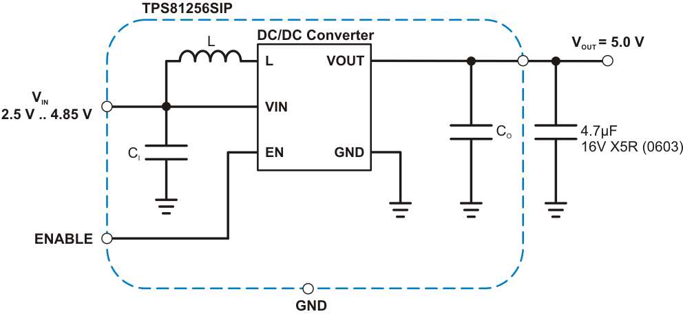
效率与负载电流间的关系
4 修订历史记录
Changes from C Revision (February 2016) to D Revision
- 更新了封装图Go
Changes from B Revision (February 2015) to C Revision
Changes from A Revision (August 2013) to B Revision
- 添加了器件信息和 ESD 额定值表、特性 说明 部分、器件功能模式、应用和实施部分、系统示例、电源建议部分、器件和文档支持部分以及机械、封装和可订购信息部分。Go
- Changed the pinout drawing to match the device orientation shown on the MECHANICAL DATA drawing. Go
- Changed 更改了 SIP 封装“俯视图”图像方向,使“YML LSB”符号和引脚 A1 正确匹配。Go
Changes from * Revision (June 2012) to A Revision
5 Device Options
| PART NUMBER(1) | OUTPUT VOLTAGE | PACKAGE MARKING
CHIP CODE |
|---|---|---|
| TPS81256 | 5.0V | TT |
(1) For the most current package and ordering information, see the Package Option Addendum at the end of this document, or see the TI website at www.ti.com.
6 Pin Configuration and Functions
Pin Functions
| PIN | I/O | DESCRIPTION | |
|---|---|---|---|
| NAME | NO. | ||
| EN | B2 | I | This is the enable pin of the device. Connecting this pin to ground forces the device into shutdown mode. Pulling this pin high enables the device. This pin must not be left floating and must be terminated. |
| GND | A1, A2, B1 | Ground pin. | |
| VIN | C1, C2 | I | Power supply input. |
| VOUT | A3, B3, C3 | O | Boost converter output. |
7 Specifications
7.1 Absolute Maximum Ratings
over operating free-air temperature range (unless otherwise noted) (1)| MIN | MAX | UNIT | |||
|---|---|---|---|---|---|
| Input voltage | Voltage at VIN(2), VOUT(2), EN(2) | –0.3 | 6 | V | |
| Input current | Continuous average current into VIN(3) | 1.05 | A | ||
| Pulsed current into VIN(4) | 1.3 | A | |||
| Power dissipation | Internally limited | ||||
| Operating temperature, TA(3)(4)(5) | –40 | 85 | °C | ||
| Operating virtual junction temperature, TJ | –40 | 150 | °C | ||
| Storage temperature, Tstg | –55 | 125 | °C | ||
(1) Stresses beyond those listed under Absolute Maximum Ratings may cause permanent damage to the device. These are stress ratings only, which do not imply functional operation of the device at these or any other conditions beyond those indicated under Recommended Operating Conditions. Exposure to absolute-maximum-rated conditions for extended periods may affect device reliability.
(2) All voltages are with respect to network ground terminal.
(3) Limit the junction and the (top side) inductor case temperature to 110°C, limit the (top side) capacitor case temperature to 85°C for 2000h operation at maximum output power. Contact TI for more details on lifetime estimation.
(4) Limit the (top side) inductor case temperature to 140°C and the (top side) capacitor temperature to 115°C for 100h operation. Contact TI for more details on lifetime estimation.
(5) In applications where high power dissipation and/or poor package thermal resistance is present, the maximum ambient temperature may have to be derated. Maximum ambient temperature (TA(max)) is dependent on the maximum operating junction temperature (TJ(max)), the maximum power dissipation of the device in the application (PD(max)), and the junction-to-ambient thermal resistance of the part/package in the application (θJA), as given by the following equation: TA(max)= TJ(max)–(θJA X PD(max)). To achieve optimum performance, it is recommended to operate the device with a maximum junction temperature of 125°C, a maximum inductor case temperature of 125°C and a maximum capacitor case temperature of 85°C.
7.2 ESD Ratings
| VALUE | UNIT | ||||
|---|---|---|---|---|---|
| V(ESD) | Electrostatic discharge | Human body model (HBM), per ANSI/ESDA/JEDEC JS-001, all pins(1) | ±2000 | V | |
| Charged device model (CDM), per JEDEC specification JESD22-C101, all pins(2) | ±1000 | ||||
| Machine Model - (MM) | ±200 | ||||
(1) JEDEC document JEP155 states that 500-V HBM allows safe manufacturing with a standard ESD control process.
(2) JEDEC document JEP157 states that 250-V CDM allows safe manufacturing with a standard ESD control process.
7.3 Recommended Operating Conditions
over operating free-air temperature range (unless otherwise noted)| MIN | NOM | MAX | UNIT | |||
|---|---|---|---|---|---|---|
| VI | Input voltage range | 2.5 | 5.5 | V | ||
| RL | Minimum resistive load for start-up (VI ≤ 4.8V) | 65 | Ω | |||
| CEXT | Output capacitance | 2 | 30 | µF | ||
| TA | Ambient temperature | –40 | 85 | °C | ||
| TJ | Operating junction temperature | –40 | 125 | °C | ||
| TCASE_IND | Operating inductor case temperature | 125 | °C | |||
| TCASE_CAP | Operating capacitor case temperature | 85 | °C | |||
7.4 Thermal Information
| THERMAL METRIC(1) | TPS81256 | UNIT | |
|---|---|---|---|
| µSIP (SIP) – 9 PINS | |||
| RθJA | Junction-to-ambient thermal resistance | 62 | °C/W |
| ψJB | Junction-to-board characterization parameter | 31 | |
| ψJT | Junction-to-case (top) thermal resistance | – | |
(1) Thermal data have been simulated with high-K board (per JEDEC standard).
7.5 Electrical Characteristics
Minimum and maximum values are at VIN = 2.5V to 5.5V, VOUT = 5.0V (or VIN, whichever is higher), EN = 1.8V, TA = –40°C to 85°C; Circuit of Parameter Measurement Information section (unless otherwise noted). Typical values are at VIN = 3.6V, VOUT = 5.0V, EN = 1.8V, TA = 25°C (unless otherwise noted).| PARAMETER | TEST CONDITIONS | MIN | TYP | MAX | UNIT | |||
|---|---|---|---|---|---|---|---|---|
| SUPPLY CURRENT | ||||||||
| IQ | Operating quiescent current into VIN(1) | IOUT = 0mA, VOUT = 5.0V, VIN = 3.6V
EN = VIN Device not switching |
30 | 50 | µA | |||
| Operating quiescent current into VOUT(1) | 7 | 20 | µA | |||||
| ISD | Shutdown current(1) | EN = GND | 0.85 | 5.0 | μA | |||
| VUVLO | Under-voltage lockout threshold | Falling | 2.0 | 2.1 | V | |||
| Hysteresis | 0.1 | V | ||||||
| ENABLE | ||||||||
| VIL | Low-level input voltage | 0.4 | V | |||||
| VIH | High-level input voltage | 1.0 | V | |||||
| Ilkg | Input leakage current | Input connected to GND or VIN | 0.5 | µA | ||||
| OUTPUT | ||||||||
| VOUT | Regulated DC output voltage | 2.5V ≤ VIN ≤ 4.85V, IOUT = 0mA
PWM operation. Open Loop |
4.92 | 5 | 5.08 | V | ||
| 3.3V ≤ VIN ≤ 4.85V, 0mA ≤ IOUT ≤ 550mA
PFM/PWM operation |
4.85 | 5 | 5.2 | V | ||||
| 2.9V ≤ VIN ≤ 4.85V, 0mA ≤ IOUT ≤ 450mA
PFM/PWM operation |
4.85 | 5 | 5.2 | V | ||||
| ΔVOUT | Power-save mode output ripple voltage | PFM operation, IOUT = 1mA | 35 | mVpk | ||||
| PWM mode output ripple voltage | PWM operation, IOUT = 200mA | 8 | mVpk | |||||
| POWER SWITCH | ||||||||
| rDS(on) | Input-to-output On-resistance | VI = 5.25 V. Device not switching | 320 | mΩ | ||||
| Ilkg | Reverse leakage current into VOUT(1) | EN = GND | 5 | µA | ||||
| ILIM | Average input current limit | EN = VIN. VIN = 3.3V | 1180 | mA | ||||
| Overtemperature protection | 140 | °C | ||||||
| Overtemperature hysteresis | 20 | °C | ||||||
| OSCILLATOR | ||||||||
| fOSC | Oscillator frequency | VIN = 3.6V, VOUT = 5.0V, IOUT = 500mA | 4 | MHz | ||||
| TIMING | ||||||||
| Start-up time | IOUT = 0mA
Time from active EN to start switching |
70 | µs | |||||
| IOUT = 0mA
Time from active EN to VOUT |
400 | µs | ||||||
(1) Maximum values can vary over lifetime due to intrinsic capacitor ageing effects. For more details, refer to Thermal and Reliability Information section.
7.6 Typical Characteristics
Table 1. Table of Graphs
| FIGURE | |||
|---|---|---|---|
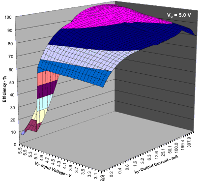
| η | Efficiency | vs Output current | Figure 1, Figure 3 |
| vs Input voltage | Figure 2 | ||
| VO | DC output voltage | vs Output current | Figure 4, Figure 5, Figure 6 |
| vs Input voltage | Figure 7 | ||
| IO | Maximum output current | vs Input voltage | Figure 8 |
| ΔVO | Peak-to-peak output ripple voltage | vs Output current | Figure 8 |
| ICC | Supply current | vs Input voltage | Figure 10 |
| ILIM | Input current | vs Output current | Figure 11 |
Table 2. Table of Animated Performance Characteristics
| VIDEO | |||
|---|---|---|---|
| AC Load Response | vs. Input Voltage | Video 1 | |
| Load Transient Response (10mA to 400mA) | vs. Input Voltage | Video 2 | |
| Load Transient Response (to 400mA) | vs. Base Load Current (2.9VIN) | Video 3 | |
| vs. Base Load Current (3.6VIN) | Video 4 | ||
| vs. Base Load Current (4.2VIN) | Video 5 | ||
| Start-Up Response | vs. Delay to Load Current (2.9VIN) | Video 6 | |
| vs. Delay to Load Current (3.6VIN) | Video 7 | ||
| vs. Delay to Load Current (4.2VIN) | Video 8 | ||
| Start-Up Response (200mA IOUT) | vs. Input Voltage | Video 9 | |
| Overload Response | vs. Input Voltage | Video 10 | |
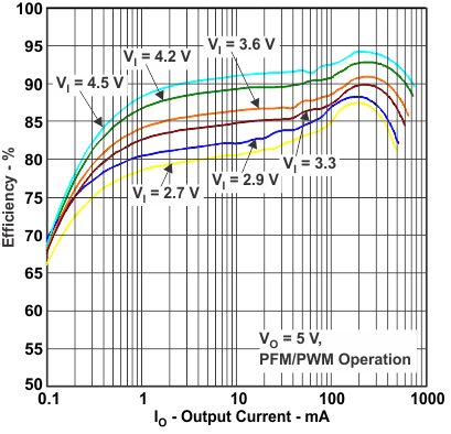 Figure 1. Efficiency vs Output Current
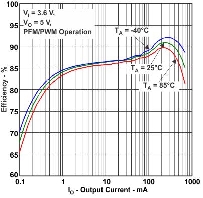 Figure 3. Efficiency vs Output Current
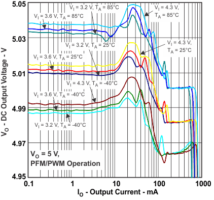 Figure 5. DC Output Voltage vs Output Current
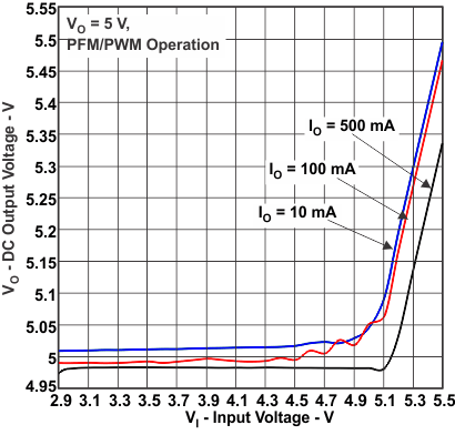 Figure 7. DC Output Voltage vs Input Voltage
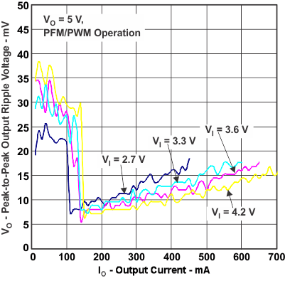 Figure 9. Peak-To-Peak Output Ripple Voltage vs Output Current
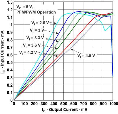
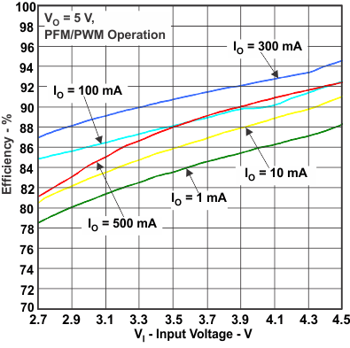 Figure 2. Efficiency vs Input Voltage
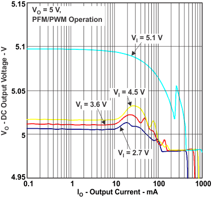 Figure 4. DC Output Voltage vs Output Current
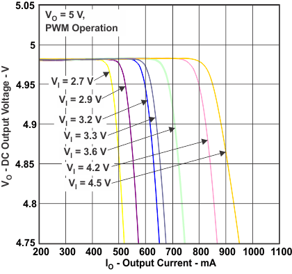 Figure 6. DC Output Voltage vs Output Current
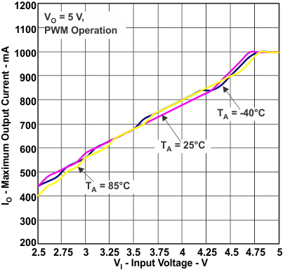 Figure 8. Maximum Output Current vs Input Voltage
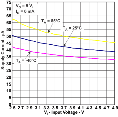 Figure 10. Supply Current vs Input Voltage
